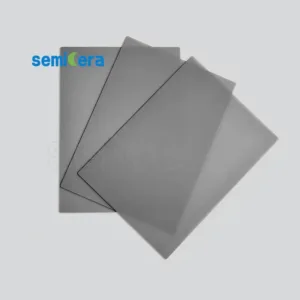
Semicera’s 8 Inch N-type SiC Wafers are at the forefront of semiconductor innovation, providing a solid base for the development of high-performance electronic devices. These wafers are designed to meet the rigorous demands of modern electronic applications, from power electronics to high-frequency circuits.
The N-type doping in these SiC wafers enhances their electrical conductivity, making them ideal for a wide range of applications, including power diodes, transistors, and amplifiers. The superior conductivity ensures minimal energy loss and efficient operation, which are critical for devices operating at high frequencies and power levels.
Semicera employs advanced manufacturing techniques to produce SiC wafers with exceptional surface uniformity and minimal defects. This level of precision is essential for applications that require consistent performance and durability, such as in aerospace, automotive, and telecommunications industries.
Incorporating Semicera’s 8 Inch N-type SiC Wafers into your production line provides a foundation for creating components that can withstand harsh environments and high temperatures. These wafers are perfect for applications in power conversion, RF technology, and other demanding fields.
Choosing Semicera’s 8 Inch N-type SiC Wafers means investing in a product that combines high-quality material science with precise engineering. Semicera is committed to advancing the capabilities of semiconductor technologies, offering solutions that enhance the efficiency and reliability of your electronic devices.
|
Rzeczy |
Produkcja |
Badania |
Atrapa |
|
Parametry kryształów |
|||
|
Polityp |
4H |
||
|
Błąd orientacji powierzchni |
4±0.15° |
||
|
Parametry elektryczne |
|||
|
Dopant |
azot typu N. |
||
|
Oporność |
0,015-0,025OHM · cm |
||
|
Parametry mechaniczne |
|||
|
Średnica |
150,0 ± 0,2 mm |
||
|
Grubość |
350 ± 25 µm |
||
|
Pierwotna płaska orientacja |
[1-100]±5° |
||
|
Pierwotna płaska długość |
47,5 ± 1,5 mm |
||
|
Wtórne mieszkanie |
Nic |
||
|
TTV |
≤5 µm |
≤10 µm |
≤15 µm |
|
LTV |
≤3 μm (5 mm*5 mm) |
≤5 μm (5 mm*5 mm) |
≤10 μm (5 mm*5 mm) |
|
Ukłon |
-15 μm ~ 15 μm |
-35 μm ~ 35 μm |
-45 μm ~ 45 μm |
|
Osnowa |
≤35 µm |
≤45 µm |
≤55 µm |
|
Chropowatość z przodu (SI-FACE) (AFM) |
RA ≤ 0,2 nm (5 μm*5 μm) |
||
|
Struktura |
|||
|
Gęstość mikropipe |
<1 ea/cm2 |
<10 ea/cm2 |
<15 ea/cm2 |
|
Zanieczyszczenia metalowe |
≤5E10atoms/cm2 |
Na |
|
|
BPD |
≤1500 EA/CM2 |
≤3000 EA/CM2 |
Na |
|
TSD |
≤500 EA/CM2 |
≤1000 EA/CM2 |
Na |
|
Jakość z przodu |
|||
|
Przód |
Si |
||
|
Wykończenie powierzchni |
SI-FACE CMP |
||
|
Cząsteczki |
≤60ea/wafel (rozmiar ≥0,3 μm) |
Na |
|
|
Zadrapania |
≤5EA/mm. Kumulatywna długość ≤ -diameter |
Skumulowana długość ≤2*średnica |
Na |
|
Skórka pomarańczowa/doły/plamy/prążki/pęknięcia/zanieczyszczenie |
Nic |
Na |
|
|
Płyty krawędziowe/wkładki/złamanie/sześciokątne płyty |
Nic |
||
|
Obszary politypowe |
Nic |
Obszar skumulowany ≤20% |
Obszar skumulowany ≤30% |
|
Przednie oznaczenie lasera |
Nic |
||
|
Jakość wstecz |
|||
|
Wstecz |
CMP-FACE CMP |
||
|
Zadrapania |
≤5EA/mm, kumulatywna długość ≤2*średnica |
Na |
|
|
Wady tylne (chipsy krawędziowe/wentylatory) |
Nic |
||
|
Chropowatość pleców |
RA ≤ 0,2 nm (5 μm*5 μm) |
||
|
Oznaczenie lasera z tyłu |
1 mm (od górnej krawędzi) |
||
|
Krawędź |
|||
|
Krawędź |
Ścięcie |
||
|
Opakowanie |
|||
|
Opakowanie |
Epi-gotowe z opakowaniem próżniowym Opakowanie kaseta z wieloma falami |
||
|
*Uwagi : „Na” oznacza, że brak wymienionych elementów, które nie wspomniane elementy mogą zapoznać się z pół-STD. |
|||