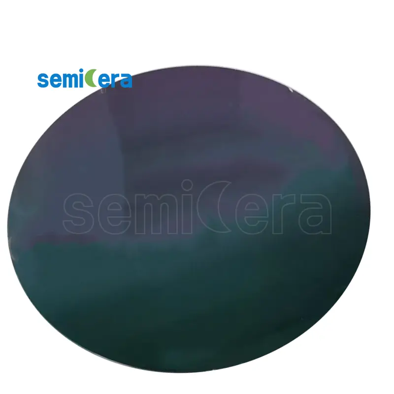
Wafel SOI SEI (krzem na izolatorze) został zaprojektowany do zapewnienia doskonałej izolacji elektrycznej i wydajności termicznej. Ta innowacyjna struktura waflowa, zawierająca krzemową warstwę na warstwie izolacyjnej, zapewnia zwiększoną wydajność urządzenia i zmniejszone zużycie energii, dzięki czemu jest idealna do różnych aplikacji zaawansowanych technologii.
Nasze wafle SOI oferują wyjątkowe korzyści dla obwodów zintegrowanych, minimalizując pasożytniczą pojemność i poprawę szybkości i wydajności urządzenia. Ma to kluczowe znaczenie dla nowoczesnej elektroniki, w której wysokiej wydajności i efektywności energetycznej są niezbędne zarówno dla zastosowań konsumenckich, jak i przemysłowych.
Semicera wykorzystuje zaawansowane techniki produkcyjne w celu wytwarzania płytek SOI o stałej jakości i niezawodności. Te wafle zapewniają doskonałą izolację termiczną, dzięki czemu są odpowiednie do stosowania w środowiskach, w których rozpraszanie ciepła jest problemem, na przykład w urządzeniach elektronicznych o dużej gęstości i systemach zarządzania energią.
Zastosowanie waflów SOI w produkcji półprzewodnikowej pozwala na opracowanie mniejszych, szybszych i bardziej niezawodnych układów. Zobowiązanie Semicera w inżynierii precyzyjnej zapewnia, że nasze wafle SOI spełniają wysokie standardy wymagane do najnowocześniejszych technologii w dziedzinach, takich jak telekomunikacja, motoryzacja i elektronika konsumpcyjna.
Wybór wafla SOI SEI, oznacza inwestowanie w produkt, który wspiera postęp technologii elektronicznych i mikroelektronicznych. Nasze wafle zostały zaprojektowane tak, aby zapewnić lepszą wydajność i trwałość, przyczyniając się do sukcesu projektów zaawansowanych technologii i zapewniając, że pozostajesz w czołówce innowacji.
|
Rzeczy |
Produkcja |
Badania |
Atrapa |
|
Parametry kryształów |
|||
|
Polityp |
4H |
||
|
Błąd orientacji powierzchni |
4±0.15° |
||
|
Parametry elektryczne |
|||
|
Dopant |
azot typu N. |
||
|
Oporność |
0,015-0,025OHM · cm |
||
|
Parametry mechaniczne |
|||
|
Średnica |
150,0 ± 0,2 mm |
||
|
Grubość |
350 ± 25 µm |
||
|
Pierwotna płaska orientacja |
[1-100]±5° |
||
|
Pierwotna płaska długość |
47,5 ± 1,5 mm |
||
|
Wtórne mieszkanie |
Nic |
||
|
TTV |
≤5 µm |
≤10 µm |
≤15 µm |
|
LTV |
≤3 μm (5 mm*5 mm) |
≤5 μm (5 mm*5 mm) |
≤10 μm (5 mm*5 mm) |
|
Ukłon |
-15 μm ~ 15 μm |
-35 μm ~ 35 μm |
-45 μm ~ 45 μm |
|
Osnowa |
≤35 µm |
≤45 µm |
≤55 µm |
|
Chropowatość z przodu (SI-FACE) (AFM) |
RA ≤ 0,2 nm (5 μm*5 μm) |
||
|
Struktura |
|||
|
Gęstość mikropipe |
<1 ea/cm2 |
<10 ea/cm2 |
<15 ea/cm2 |
|
Zanieczyszczenia metalowe |
≤5E10atoms/cm2 |
Na |
|
|
BPD |
≤1500 EA/CM2 |
≤3000 EA/CM2 |
Na |
|
TSD |
≤500 EA/CM2 |
≤1000 EA/CM2 |
Na |
|
Jakość z przodu |
|||
|
Przód |
Si |
||
|
Wykończenie powierzchni |
SI-FACE CMP |
||
|
Cząsteczki |
≤60ea/wafel (rozmiar ≥0,3 μm) |
Na |
|
|
Zadrapania |
≤5EA/mm. Kumulatywna długość ≤ -diameter |
Skumulowana długość ≤2*średnica |
Na |
|
Skórka pomarańczowa/doły/plamy/prążki/pęknięcia/zanieczyszczenie |
Nic |
Na |
|
|
Płyty krawędziowe/wkładki/złamanie/sześciokątne płyty |
Nic |
||
|
Obszary politypowe |
Nic |
Obszar skumulowany ≤20% |
Obszar skumulowany ≤30% |
|
Przednie oznaczenie lasera |
Nic |
||
|
Jakość wstecz |
|||
|
Wstecz |
CMP-FACE CMP |
||
|
Zadrapania |
≤5EA/mm, kumulatywna długość ≤2*średnica |
Na |
|
|
Wady tylne (chipsy krawędziowe/wentylatory) |
Nic |
||
|
Chropowatość pleców |
RA ≤ 0,2 nm (5 μm*5 μm) |
||
|
Oznaczenie lasera z tyłu |
1 mm (od górnej krawędzi) |
||
|
Krawędź |
|||
|
Krawędź |
Ścięcie |
||
|
Opakowanie |
|||
|
Opakowanie |
Epi-gotowe z opakowaniem próżniowym Opakowanie kaseta z wieloma falami |
||
|
*Uwagi : „Na” oznacza, że brak wymienionych elementów, które nie wspomniane elementy mogą zapoznać się z pół-STD. |
|||


