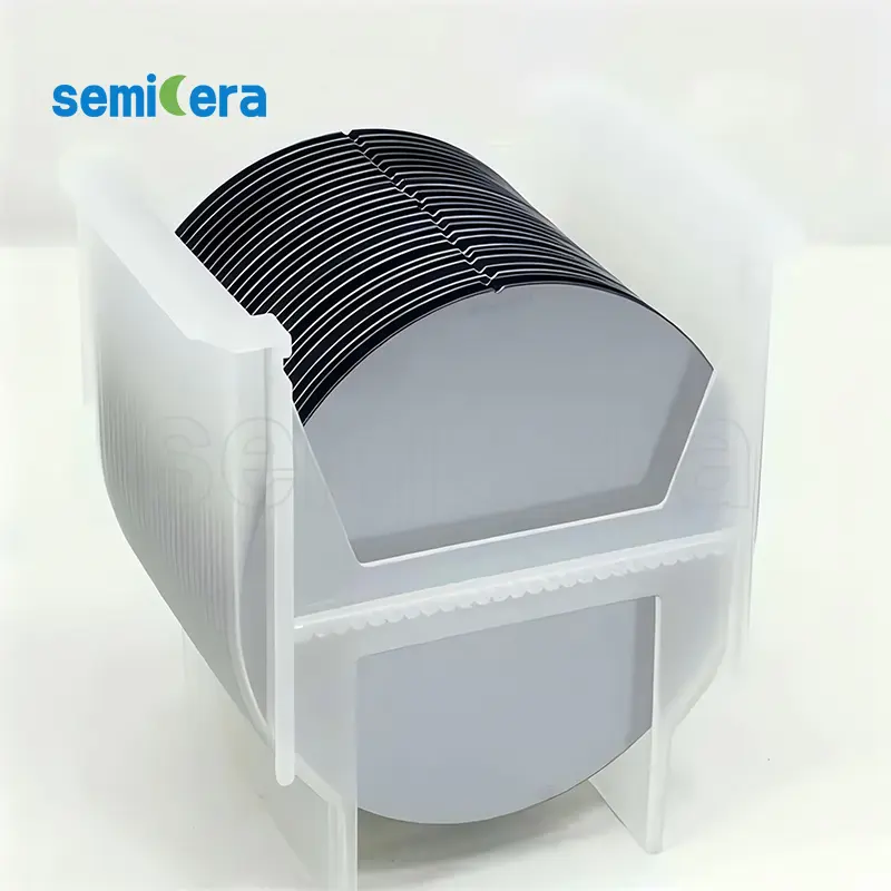
Semicera introduces the Wafer Cassette Carrier, a critical solution for the secure and efficient handling of semiconductor wafers. This carrier is engineered to meet the stringent requirements of the semiconductor industry, ensuring the protection and integrity of your wafers throughout the manufacturing process.
Key Features:
• Robust Construction: . Wafer Cassette Carrier is built from high-quality, durable materials that withstand the rigors of semiconductor environments, providing reliable protection against contamination and physical damage.
• Precise Alignment: Designed for precise wafer alignment, this carrier ensures that wafers are securely held in place, minimizing the risk of misalignment or damage during transport.
• Easy Handling: Ergonomically designed for ease of use, the carrier simplifies the loading and unloading process, improving workflow efficiency in cleanroom environments.
• Compatibility: Compatible with a wide range of wafer sizes and types, making it versatile for various semiconductor manufacturing needs.
Experience unparalleled protection and convenience with Semicera’s Wafer Cassette Carrier. Our carrier is designed to meet the highest standards of semiconductor manufacturing, ensuring your wafers remain in pristine condition from start to finish. Trust Semicera to deliver the quality and reliability you need for your most critical processes.
|
Rzeczy |
Produkcja |
Badania |
Atrapa |
|
Parametry kryształów |
|||
|
Polityp |
4H |
||
|
Błąd orientacji powierzchni |
4±0.15° |
||
|
Parametry elektryczne |
|||
|
Dopant |
azot typu N. |
||
|
Oporność |
0,015-0,025OHM · cm |
||
|
Parametry mechaniczne |
|||
|
Średnica |
150,0 ± 0,2 mm |
||
|
Grubość |
350 ± 25 µm |
||
|
Pierwotna płaska orientacja |
[1-100]±5° |
||
|
Pierwotna płaska długość |
47,5 ± 1,5 mm |
||
|
Wtórne mieszkanie |
Nic |
||
|
TTV |
≤5 µm |
≤10 µm |
≤15 µm |
|
LTV |
≤3 μm (5 mm*5 mm) |
≤5 μm (5 mm*5 mm) |
≤10 μm (5 mm*5 mm) |
|
Ukłon |
-15 μm ~ 15 μm |
-35 μm ~ 35 μm |
-45 μm ~ 45 μm |
|
Osnowa |
≤35 µm |
≤45 µm |
≤55 µm |
|
Chropowatość z przodu (SI-FACE) (AFM) |
RA ≤ 0,2 nm (5 μm*5 μm) |
||
|
Struktura |
|||
|
Gęstość mikropipe |
<1 ea/cm2 |
<10 ea/cm2 |
<15 ea/cm2 |
|
Zanieczyszczenia metalowe |
≤5E10atoms/cm2 |
Na |
|
|
BPD |
≤1500 EA/CM2 |
≤3000 EA/CM2 |
Na |
|
TSD |
≤500 EA/CM2 |
≤1000 EA/CM2 |
Na |
|
Jakość z przodu |
|||
|
Przód |
Si |
||
|
Wykończenie powierzchni |
SI-FACE CMP |
||
|
Cząsteczki |
≤60ea/wafel (rozmiar ≥0,3 μm) |
Na |
|
|
Zadrapania |
≤5EA/mm. Kumulatywna długość ≤ -diameter |
Skumulowana długość ≤2*średnica |
Na |
|
Skórka pomarańczowa/doły/plamy/prążki/pęknięcia/zanieczyszczenie |
Nic |
Na |
|
|
Płyty krawędziowe/wkładki/złamanie/sześciokątne płyty |
Nic |
||
|
Obszary politypowe |
Nic |
Obszar skumulowany ≤20% |
Obszar skumulowany ≤30% |
|
Przednie oznaczenie lasera |
Nic |
||
|
Jakość wstecz |
|||
|
Wstecz |
CMP-FACE CMP |
||
|
Zadrapania |
≤5EA/mm, kumulatywna długość ≤2*średnica |
Na |
|
|
Wady tylne (chipsy krawędziowe/wentylatory) |
Nic |
||
|
Chropowatość pleców |
RA ≤ 0,2 nm (5 μm*5 μm) |
||
|
Oznaczenie lasera z tyłu |
1 mm (od górnej krawędzi) |
||
|
Krawędź |
|||
|
Krawędź |
Ścięcie |
||
|
Opakowanie |
|||
|
Opakowanie |
Epi-gotowe z opakowaniem próżniowym Opakowanie kaseta z wieloma falami |
||
|
*Uwagi : „Na” oznacza, że brak wymienionych elementów, które nie wspomniane elementy mogą zapoznać się z pół-STD. |
|||


