تحتوي المادة البلورية المفردة على كربيد السيليكون (SIC) على عرض فجوة كبيرة في النطاق (~ SI 3 مرات) ، والتوصيل الحراري العالي (~ Si 3.3 مرات أو GaAs 10 مرات) ، ومعدل ترحيل تشبع الإلكترون العالي (~ SI 2.5 مرة) ، وحقل كهربائي عالي الانهيار (~ Si 10 مرات أو غواس 5 مرات) وغيرها من الخصائص غير المتميزة.
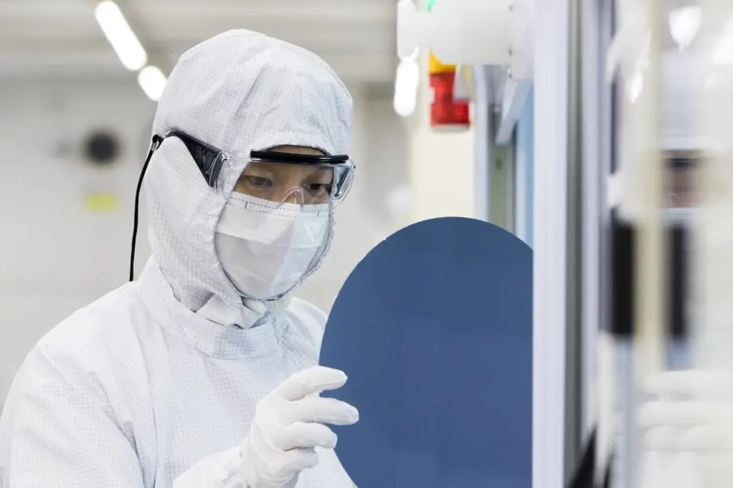
يمكن أن تزود شركة Semicera Energy للعملاء بتوصيل عالي الجودة (موصل) ، وشبه العذبة (شبه العذبة) ، و HPSI (نقاء عالي نقاء) الركيزة كربيد السيليكون ؛ بالإضافة إلى ذلك ، يمكننا تزويد العملاء بألواح سليكون محورية متجانسة وغير متجانسة ؛ يمكننا أيضًا تخصيص الورقة الفوقية وفقًا للاحتياجات المحددة للعملاء ، ولا توجد كمية أدنى للطلب.
|
أغراض |
إنتاج |
بحث |
دمية |
|
المعلمات البلورية |
|||
|
polytype |
4H |
||
|
خطأ في اتجاه السطح |
<11-20 >4±0.15° |
||
|
المعلمات الكهربائية |
|||
|
Dopant |
نيتروجين من النوع |
||
|
المقاومة |
0.015-0.025ohm·cm |
||
|
المعلمات الميكانيكية |
|||
|
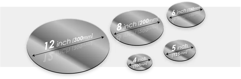
قطر |
99.5 – 100mm |
||
|
سماكة |
350±25 μm |
||
|
الاتجاه المسطح الأولي |
[1-100]±5° |
||
|
طول مسطح أساسي |
32.5±1.5mm |
||
|
Secondary flat position |
90° CW from primary flat ±5°. silicon face up |
||
|
Secondary flat length |
18±1.5mm |
||
|
TTV |
≤5 μm |
≤10 μm |
≤20 μm |
|
LTV |
≤2 μm(5mm*5mm) |
≤5 μm(5mm*5mm) |
نا |
|
قَوس |
-15μm ~ 15μm |
-35μm ~ 35μm |
-45μm ~ 45μm |
|
الاعوجاج |
≤20 μm |
≤45 μm |
≤50 μm |
|
الخشونة الأمامية (si-face) (AFM) |
Ra≤0.2nm (5μm*5μm) |
||
|
بناء |
|||
|
كثافة micropipe |
≤1 ea/cm2 |
≤5 ea/cm2 |
≤10 ea/cm2 |
|
الشوائب المعدنية |
≤5E10atoms/cm2 |
نا |
|
|
BPD |
≤1500 ea/cm2 |
≤3000 ea/cm2 |
نا |
|
TSD |
≤500 ea/cm2 |
≤1000 ea/cm2 |
نا |
|
الجودة الأمامية |
|||
|
أمام |
سي |
||
|
الانتهاء من السطح |
Si-Face CMP |
||
|
الجزيئات |
≤60ea/wafer (size≥0.3μm) |
نا |
|
|
الخدوش |
≤2ea/mm. Cumulative length ≤Diameter |
Cumulative length≤2*Diameter |
نا |
|
قشر البرتقال/الحفر/البقع/الدماغ/الشقوق/التلوث |
لا أحد |
نا |
|
|
رقائق الحافة/المسافات البادئة/الكسر/الألواح السداسية |
لا أحد |
نا |
|
|
المناطق polytype |
لا أحد |
Cumulative area≤20% |
Cumulative area≤30% |
|
وضع علامة ليزر الأمامية |
لا أحد |
||
|
جودة الظهر |
|||
|
الانتهاء من الظهر |
C-Face CMP |
||
|
الخدوش |
≤5ea/mm,Cumulative length≤2*Diameter |
نا |
|
|
عيوب الظهر (رقائق الحافة/المسافات البادئة) |
لا أحد |
||
|
خشونة الظهر |
Ra≤0.2nm (5μm*5μm) |
||
|
عودة ليزر العلامات |
1 مم (من الحافة العليا) |
||
|
حافة |
|||
|
حافة |
شامفر |
||
|
التغليف |
|||
|
التغليف |
The inner bag is filled with nitrogen and the outer bag is vacuumed. Multi-wafer cassette, epi-ready. |
||
|
*الملاحظات : "NA" تعني عدم وجود عناصر طلب لم يتم ذكرها قد تشير إلى Semi. |
|||