تحتوي المادة البلورية المفردة على كربيد السيليكون (SIC) على عرض فجوة كبيرة في النطاق (~ SI 3 مرات) ، والتوصيل الحراري العالي (~ Si 3.3 مرات أو GaAs 10 مرات) ، ومعدل ترحيل تشبع الإلكترون العالي (~ SI 2.5 مرة) ، وحقل كهربائي عالي الانهيار (~ Si 10 مرات أو غواس 5 مرات) وغيرها من الخصائص غير المتميزة.
تشمل مواد أشباه الموصلات الجيل الثالث بشكل أساسي SIC ، GAN ، Diamond ، إلخ ، لأن عرض فجوة النطاق (EG) أكبر من أو يساوي 2.3 فولت الإلكترون (EV) ، والمعروف أيضًا باسم مواد أشباه الموصلات الفجوة على نطاق واسع. مقارنةً بمواد أشباه الموصلات من الجيل الأول والثاني ، فإن مواد أشباه الموصلات الجيل الثالث لها مزايا الموصلية الحرارية العالية ، والجقل الكهربائي العالي ، ومعدل ترحيل الإلكترون المشبع المرتفع ، وارتفاع طاقة الترابط ، والتي يمكن أن تلبي المتطلبات الجديدة للتكنولوجيا الإلكترونية الحديثة لدرجة الحرارة المرتفعة ، والضغط العالي ، وارتفاع التردد ، وظروف الإشعاع وغيرها من الحالات. لديها آفاق تطبيق مهمة في مجالات الدفاع الوطني ، الطيران ، الفضاء ، استكشاف النفط ، التخزين البصري ، وما إلى ذلك ، ويمكن أن تقلل من فقدان الطاقة بأكثر من 50% في العديد من الصناعات الاستراتيجية مثل اتصالات النطاق العريض ، والطاقة الشمسية ، والسيارات المصنعة للتكنولوجيا.
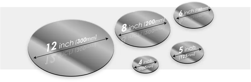
يمكن أن تزود شركة Semicera Energy للعملاء بتوصيل عالي الجودة (موصل) ، وشبه العذبة (شبه العذبة) ، و HPSI (نقاء عالي نقاء) الركيزة كربيد السيليكون ؛ بالإضافة إلى ذلك ، يمكننا تزويد العملاء بألواح سليكون محورية متجانسة وغير متجانسة ؛ يمكننا أيضًا تخصيص الورقة الفوقية وفقًا للاحتياجات المحددة للعملاء ، ولا توجد كمية أدنى للطلب.
|
أغراض |
إنتاج |
بحث |
دمية |
|
المعلمات البلورية |
|||
|
polytype |
4H |
||
|
خطأ في اتجاه السطح |
<11-20 >4±0.15° |
||
|
المعلمات الكهربائية |
|||
|
Dopant |
نيتروجين من النوع |
||
|
المقاومة |
0.015-0.025ohm·cm |
||
|
المعلمات الميكانيكية |
|||
|
قطر |
150.0±0.2mm |
||
|
سماكة |
350±25 μm |
||
|
الاتجاه المسطح الأولي |
[1-100]±5° |
||
|
طول مسطح أساسي |
47.5±1.5mm |
||
|
شقة ثانوية |
لا أحد |
||
|
TTV |
≤5 μm |
≤10 μm |
≤15 μm |
|
LTV |
≤3 μm(5mm*5mm) |
≤5 μm(5mm*5mm) |
≤10 μm(5mm*5mm) |
|
قَوس |
-15μm ~ 15μm |
-35μm ~ 35μm |
-45μm ~ 45μm |
|
الاعوجاج |
≤35 μm |
≤45 μm |
≤55 μm |
|
الخشونة الأمامية (si-face) (AFM) |
Ra≤0.2nm (5μm*5μm) |
||
|
بناء |
|||
|
كثافة micropipe |
<1 EA/CM2 |
<10 EA/CM2 |
<15 EA/CM2 |
|
الشوائب المعدنية |
≤5E10atoms/cm2 |
نا |
|
|
BPD |
≤1500 ea/cm2 |
≤3000 ea/cm2 |
نا |
|
TSD |
≤500 ea/cm2 |
≤1000 ea/cm2 |
نا |
|
الجودة الأمامية |
|||
|
أمام |
سي |
||
|
الانتهاء من السطح |
Si-Face CMP |
||
|
الجزيئات |
≤60ea/wafer (size≥0.3μm) |
نا |
|
|
الخدوش |
≤5ea/mm. Cumulative length ≤Diameter |
Cumulative length≤2*Diameter |
نا |
|
قشر البرتقال/الحفر/البقع/الدماغ/الشقوق/التلوث |
لا أحد |
نا |
|
|
رقائق الحافة/المسافات البادئة/الكسر/الألواح السداسية |
لا أحد |
||
|
المناطق polytype |
لا أحد |
Cumulative area≤20% |
Cumulative area≤30% |
|
وضع علامة ليزر الأمامية |
لا أحد |
||
|
جودة الظهر |
|||
|
الانتهاء من الظهر |
C-Face CMP |
||
|
الخدوش |
≤5ea/mm,Cumulative length≤2*Diameter |
نا |
|
|
عيوب الظهر (رقائق الحافة/المسافات البادئة) |
لا أحد |
||
|
خشونة الظهر |
Ra≤0.2nm (5μm*5μm) |
||
|
عودة ليزر العلامات |
1 مم (من الحافة العليا) |
||
|
حافة |
|||
|
حافة |
شامفر |
||
|
التغليف |
|||
|
التغليف |
جاهز لـ EPI مع تغليف فراغ عبوات الكاسيت متعددة الفرس |
||
|
*الملاحظات : "NA" تعني عدم وجود عناصر طلب لم يتم ذكرها قد تشير إلى Semi. |
|||