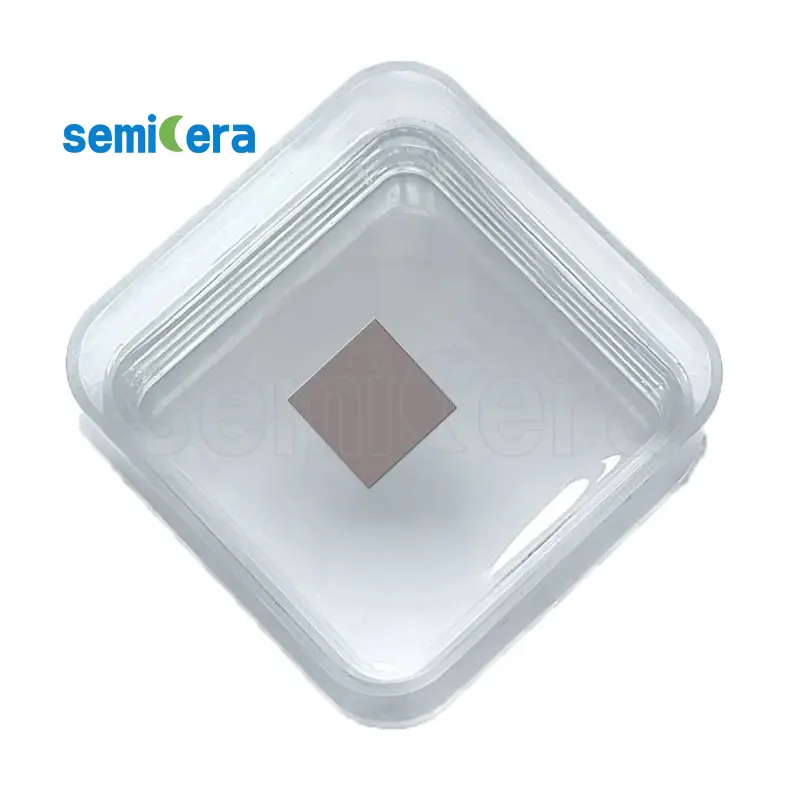
semicera's 10 × 10 مم من الركيزة الألمنيوم M-Plane is meticulously designed to meet the exacting requirements of advanced optoelectronic applications. This substrate features a nonpolar M-plane orientation, which is critical for reducing polarization effects in devices such as LEDs and laser diodes, leading to enhanced performance and efficiency.
ال 10 × 10 مم من الركيزة الألمنيوم M-Plane is crafted with exceptional crystalline quality, ensuring minimal defect densities and superior structural integrity. This makes it an ideal choice for the epitaxial growth of high-quality III-nitride films, which are essential for the development of next-generation optoelectronic devices.
Semicera’s precision engineering ensures that each 10 × 10 مم من الركيزة الألمنيوم M-Plane offers consistent thickness and surface flatness, which are crucial for uniform film deposition and device fabrication. Additionally, the substrate’s compact size makes it suitable for both research and production environments, allowing for flexible use in a variety of applications. With its excellent thermal and chemical stability, this substrate provides a reliable foundation for the development of cutting-edge optoelectronic technologies.
|
أغراض |
إنتاج |
بحث |
دمية |
|
المعلمات البلورية |
|||
|
polytype |
4H |
||
|
خطأ في اتجاه السطح |
4±0.15° |
||
|
المعلمات الكهربائية |
|||
|
Dopant |
نيتروجين من النوع |
||
|
المقاومة |
0.015-0.025OHM · سم |
||
|
المعلمات الميكانيكية |
|||
|
قطر |
150.0 ± 0.2mm |
||
|
سماكة |
350 ± 25 ميكرون |
||
|
الاتجاه المسطح الأولي |
[1-100]±5° |
||
|
طول مسطح أساسي |
47.5 ± 1.5mm |
||
|
شقة ثانوية |
لا أحد |
||
|
TTV |
≤5 ميكرون |
≤10 ميكرون |
≤15 ميكرون |
|
LTV |
≤3 ميكرون (5 ملم*5 ملم) |
≤5 ميكرون (5 ملم*5 ملم) |
≤10 ميكرون (5 ملم*5 ملم) |
|
قَوس |
-15μm ~ 15μm |
-35μm ~ 35μm |
-45μm ~ 45μm |
|
الاعوجاج |
≤35 ميكرون |
≤45 ميكرون |
≤55 ميكرون |
|
الخشونة الأمامية (si-face) (AFM) |
Ra≤0.2nm (5μm*5μm) |
||
|
بناء |
|||
|
كثافة micropipe |
<1 EA/CM2 |
<10 EA/CM2 |
<15 EA/CM2 |
|
الشوائب المعدنية |
≤5E10atoms/cm2 |
نا |
|
|
BPD |
≤1500 EA/CM2 |
≤3000 EA/CM2 |
نا |
|
TSD |
≤500 EA/CM2 |
≤1000 EA/CM2 |
نا |
|
الجودة الأمامية |
|||
|
أمام |
سي |
||
|
الانتهاء من السطح |
Si-Face CMP |
||
|
الجزيئات |
≤60A/WEFR (SIZE 30.3μM) |
نا |
|
|
الخدوش |
≤5ea/مم. الطول التراكمي ≤Diameter |
الطول التراكمي ≤2*القطر |
نا |
|
قشر البرتقال/الحفر/البقع/الدماغ/الشقوق/التلوث |
لا أحد |
نا |
|
|
رقائق الحافة/المسافات البادئة/الكسر/الألواح السداسية |
لا أحد |
||
|
المناطق polytype |
لا أحد |
منطقة تراكمية 20% |
التراكمية منطقة ≤30% |
|
وضع علامة ليزر الأمامية |
لا أحد |
||
|
جودة الظهر |
|||
|
الانتهاء من الظهر |
C-Face CMP |
||
|
الخدوش |
≤5EA/MM ، الطول التراكمي ≤2*القطر |
نا |
|
|
عيوب الظهر (رقائق الحافة/المسافات البادئة) |
لا أحد |
||
|
خشونة الظهر |
Ra≤0.2nm (5μm*5μm) |
||
|
عودة ليزر العلامات |
1 مم (من الحافة العليا) |
||
|
حافة |
|||
|
حافة |
شامفر |
||
|
التغليف |
|||
|
التغليف |
جاهز لـ EPI مع تغليف فراغ عبوات الكاسيت متعددة الفرس |
||
|
*الملاحظات : "NA" تعني عدم وجود عناصر طلب لم يتم ذكرها قد تشير إلى Semi. |
|||


