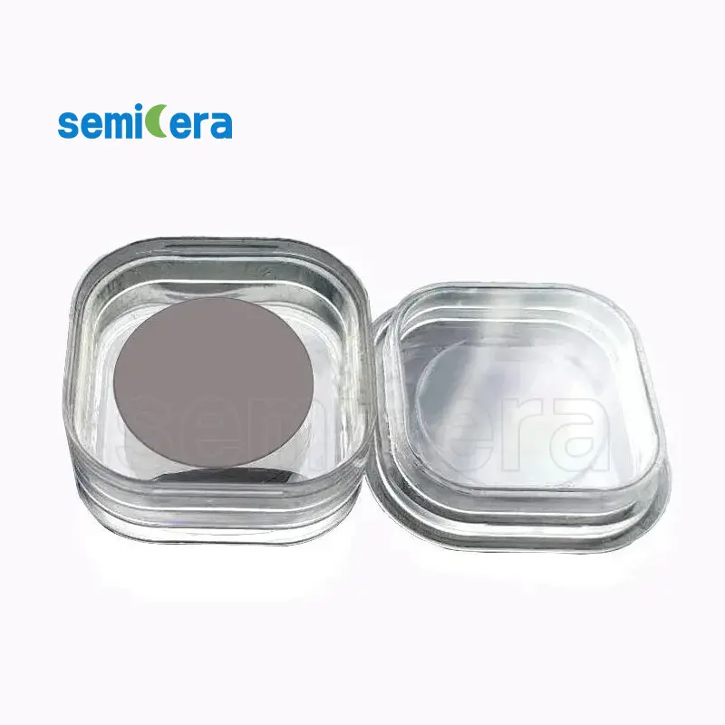
شبه is proud to present the 30mm Aluminum Nitride Wafer Substrate, a top-tier material engineered to meet the stringent demands of modern electronic and optoelectronic applications. Aluminum Nitride (AlN) substrates are renowned for their outstanding thermal conductivity and electrical insulation properties, making them an ideal choice for high-performance devices.
الميزات الرئيسية:
• Exceptional Thermal Conductivity: The 30mm Aluminum Nitride Wafer Substrate boasts a thermal conductivity of up to 170 W/mK, significantly higher than other substrate materials, ensuring efficient heat dissipation in high-power applications.
• High Electrical Insulation: With excellent electrical insulating properties, this substrate minimizes cross-talk and signal interference, making it ideal for RF and microwave applications.
• Mechanical Strength: The 30mm Aluminum Nitride Wafer Substrate offers superior mechanical strength and stability, ensuring durability and reliability even under rigorous operating conditions.
• التطبيقات متعددة الاستخدامات: This substrate is perfect for use in high-power LEDs, laser diodes, and RF components, providing a robust and reliable foundation for your most demanding projects.
• Precision Fabrication: Semicera ensures that each wafer substrate is fabricated with the highest precision, offering uniform thickness and surface quality to meet the exacting standards of advanced electronic devices.
Maximize the efficiency and reliability of your devices with Semicera’s 30mm Aluminum Nitride Wafer Substrate. Our substrates are designed to deliver superior performance, ensuring that your electronic and optoelectronic systems operate at their best. Trust Semicera for cutting-edge materials that lead the industry in quality and innovation.
|
أغراض |
إنتاج |
بحث |
دمية |
|
المعلمات البلورية |
|||
|
polytype |
4H |
||
|
خطأ في اتجاه السطح |
4±0.15° |
||
|
المعلمات الكهربائية |
|||
|
Dopant |
نيتروجين من النوع |
||
|
المقاومة |
0.015-0.025OHM · سم |
||
|
المعلمات الميكانيكية |
|||
|
قطر |
150.0 ± 0.2mm |
||
|
سماكة |
350 ± 25 ميكرون |
||
|
الاتجاه المسطح الأولي |
[1-100]±5° |
||
|
طول مسطح أساسي |
47.5 ± 1.5mm |
||
|
شقة ثانوية |
لا أحد |
||
|
TTV |
≤5 ميكرون |
≤10 ميكرون |
≤15 ميكرون |
|
LTV |
≤3 ميكرون (5 ملم*5 ملم) |
≤5 ميكرون (5 ملم*5 ملم) |
≤10 ميكرون (5 ملم*5 ملم) |
|
قَوس |
-15μm ~ 15μm |
-35μm ~ 35μm |
-45μm ~ 45μm |
|
الاعوجاج |
≤35 ميكرون |
≤45 ميكرون |
≤55 ميكرون |
|
الخشونة الأمامية (si-face) (AFM) |
Ra≤0.2nm (5μm*5μm) |
||
|
بناء |
|||
|
كثافة micropipe |
<1 EA/CM2 |
<10 EA/CM2 |
<15 EA/CM2 |
|
الشوائب المعدنية |
≤5E10atoms/cm2 |
نا |
|
|
BPD |
≤1500 EA/CM2 |
≤3000 EA/CM2 |
نا |
|
TSD |
≤500 EA/CM2 |
≤1000 EA/CM2 |
نا |
|
الجودة الأمامية |
|||
|
أمام |
سي |
||
|
الانتهاء من السطح |
Si-Face CMP |
||
|
الجزيئات |
≤60A/WEFR (SIZE 30.3μM) |
نا |
|
|
الخدوش |
≤5ea/مم. الطول التراكمي ≤Diameter |
الطول التراكمي ≤2*القطر |
نا |
|
قشر البرتقال/الحفر/البقع/الدماغ/الشقوق/التلوث |
لا أحد |
نا |
|
|
رقائق الحافة/المسافات البادئة/الكسر/الألواح السداسية |
لا أحد |
||
|
المناطق polytype |
لا أحد |
منطقة تراكمية 20% |
التراكمية منطقة ≤30% |
|
وضع علامة ليزر الأمامية |
لا أحد |
||
|
جودة الظهر |
|||
|
الانتهاء من الظهر |
C-Face CMP |
||
|
الخدوش |
≤5EA/MM ، الطول التراكمي ≤2*القطر |
نا |
|
|
عيوب الظهر (رقائق الحافة/المسافات البادئة) |
لا أحد |
||
|
خشونة الظهر |
Ra≤0.2nm (5μm*5μm) |
||
|
عودة ليزر العلامات |
1 مم (من الحافة العليا) |
||
|
حافة |
|||
|
حافة |
شامفر |
||
|
التغليف |
|||
|
التغليف |
جاهز لـ EPI مع تغليف فراغ عبوات الكاسيت متعددة الفرس |
||
|
*الملاحظات : "NA" تعني عدم وجود عناصر طلب لم يتم ذكرها قد تشير إلى Semi. |
|||


