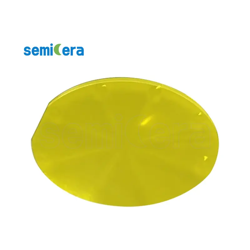
Semicera 3C-SiC Wafer Substrates are engineered to provide a robust platform for next-generation power electronics and high-frequency devices. With superior thermal properties and electrical characteristics, these substrates are designed to meet the demanding requirements of modern technology.
The 3C-SiC (Cubic Silicon Carbide) structure of Semicera Wafer Substrates offers unique advantages, including higher thermal conductivity and a lower thermal expansion coefficient compared to other semiconductor materials. This makes them an excellent choice for devices operating under extreme temperatures and high-power conditions.
With a high electrical breakdown voltage and superior chemical stability, Semicera 3C-SiC Wafer Substrates ensure long-lasting performance and reliability. These properties are critical for applications such as high-frequency radar, solid-state lighting, and power inverters, where efficiency and durability are paramount.
Semicera’s commitment to quality is reflected in the meticulous manufacturing process of their 3C-SiC Wafer Substrates, ensuring uniformity and consistency across every batch. This precision contributes to the overall performance and longevity of the electronic devices built upon them.
By choosing Semicera 3C-SiC Wafer Substrates, manufacturers gain access to a cutting-edge material that enables the development of smaller, faster, and more efficient electronic components. Semicera continues to support technological innovation by providing reliable solutions that meet the evolving demands of the semiconductor industry.
|
أغراض |
إنتاج |
بحث |
دمية |
|
المعلمات البلورية |
|||
|
polytype |
4H |
||
|
خطأ في اتجاه السطح |
4±0.15° |
||
|
المعلمات الكهربائية |
|||
|
Dopant |
نيتروجين من النوع |
||
|
المقاومة |
0.015-0.025OHM · سم |
||
|
المعلمات الميكانيكية |
|||
|
قطر |
150.0 ± 0.2mm |
||
|
سماكة |
350 ± 25 ميكرون |
||
|
الاتجاه المسطح الأولي |
[1-100]±5° |
||
|
طول مسطح أساسي |
47.5 ± 1.5mm |
||
|
شقة ثانوية |
لا أحد |
||
|
TTV |
≤5 ميكرون |
≤10 ميكرون |
≤15 ميكرون |
|
LTV |
≤3 ميكرون (5 ملم*5 ملم) |
≤5 ميكرون (5 ملم*5 ملم) |
≤10 ميكرون (5 ملم*5 ملم) |
|
قَوس |
-15μm ~ 15μm |
-35μm ~ 35μm |
-45μm ~ 45μm |
|
الاعوجاج |
≤35 ميكرون |
≤45 ميكرون |
≤55 ميكرون |
|
الخشونة الأمامية (si-face) (AFM) |
Ra≤0.2nm (5μm*5μm) |
||
|
بناء |
|||
|
كثافة micropipe |
<1 EA/CM2 |
<10 EA/CM2 |
<15 EA/CM2 |
|
الشوائب المعدنية |
≤5E10atoms/cm2 |
نا |
|
|
BPD |
≤1500 EA/CM2 |
≤3000 EA/CM2 |
نا |
|
TSD |
≤500 EA/CM2 |
≤1000 EA/CM2 |
نا |
|
الجودة الأمامية |
|||
|
أمام |
سي |
||
|
الانتهاء من السطح |
Si-Face CMP |
||
|
الجزيئات |
≤60A/WEFR (SIZE 30.3μM) |
نا |
|
|
الخدوش |
≤5ea/مم. الطول التراكمي ≤Diameter |
الطول التراكمي ≤2*القطر |
نا |
|
قشر البرتقال/الحفر/البقع/الدماغ/الشقوق/التلوث |
لا أحد |
نا |
|
|
رقائق الحافة/المسافات البادئة/الكسر/الألواح السداسية |
لا أحد |
||
|
المناطق polytype |
لا أحد |
منطقة تراكمية 20% |
التراكمية منطقة ≤30% |
|
وضع علامة ليزر الأمامية |
لا أحد |
||
|
جودة الظهر |
|||
|
الانتهاء من الظهر |
C-Face CMP |
||
|
الخدوش |
≤5EA/MM ، الطول التراكمي ≤2*القطر |
نا |
|
|
عيوب الظهر (رقائق الحافة/المسافات البادئة) |
لا أحد |
||
|
خشونة الظهر |
Ra≤0.2nm (5μm*5μm) |
||
|
عودة ليزر العلامات |
1 مم (من الحافة العليا) |
||
|
حافة |
|||
|
حافة |
شامفر |
||
|
التغليف |
|||
|
التغليف |
جاهز لـ EPI مع تغليف فراغ عبوات الكاسيت متعددة الفرس |
||
|
*الملاحظات : "NA" تعني عدم وجود عناصر طلب لم يتم ذكرها قد تشير إلى Semi. |
|||


