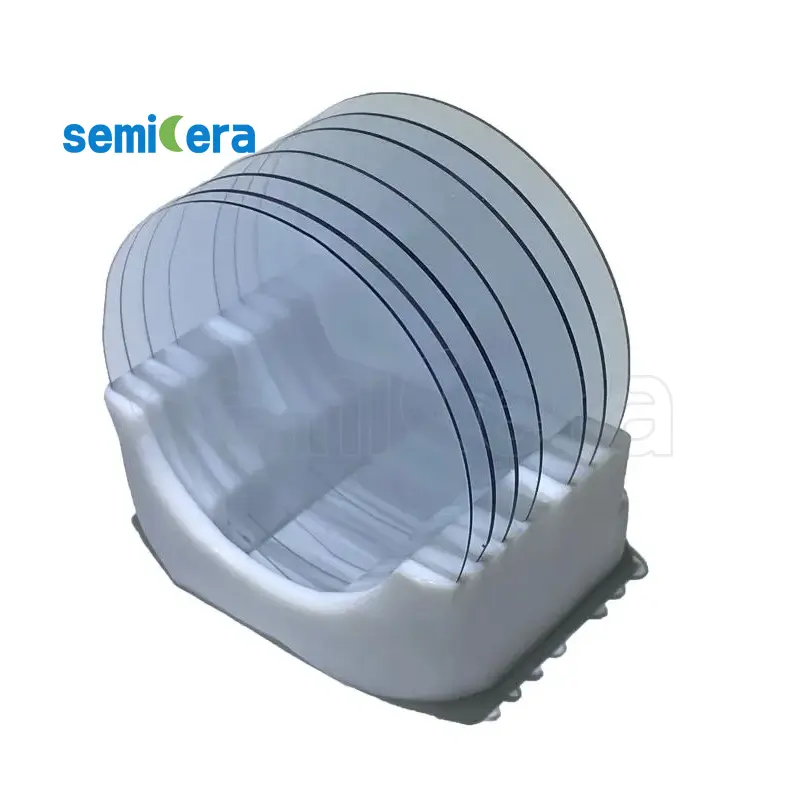
شبه proudly introduces its 4″ Gallium Oxide Substrates, a groundbreaking material engineered to meet the growing demands of high-performance semiconductor devices. Gallium Oxide (Ga2O3) substrates offer an ultra-wide bandgap, making them ideal for next-generation power electronics, UV optoelectronics, and high-frequency devices.
الميزات الرئيسية:
• Ultra-Wide Bandgap: The 4″ Gallium Oxide Substrates boast a bandgap of approximately 4.8 eV, allowing for exceptional voltage and temperature tolerance, significantly outperforming traditional semiconductor materials like silicon.
• High Breakdown Voltage: These substrates enable devices to operate at higher voltages and powers, making them perfect for high-voltage applications in power electronics.
• Superior Thermal Stability: Gallium Oxide substrates offer excellent thermal conductivity, ensuring stable performance under extreme conditions, ideal for use in demanding environments.
• High Material Quality: With low defect densities and high crystal quality, these substrates ensure reliable and consistent performance, enhancing the efficiency and durability of your devices.
• Versatile Application: Suitable for a wide range of applications, including power transistors, Schottky diodes, and UV-C LED devices, enabling innovations in both power and optoelectronic fields.
Explore the future of semiconductor technology with Semicera’s 4″ Gallium Oxide Substrates. Our substrates are designed to support the most advanced applications, providing the reliability and efficiency required for today’s cutting-edge devices. Trust Semicera for quality and innovation in your semiconductor materials.
|
أغراض |
إنتاج |
بحث |
دمية |
|
المعلمات البلورية |
|||
|
polytype |
4H |
||
|
خطأ في اتجاه السطح |
4±0.15° |
||
|
المعلمات الكهربائية |
|||
|
Dopant |
نيتروجين من النوع |
||
|
المقاومة |
0.015-0.025OHM · سم |
||
|
المعلمات الميكانيكية |
|||
|
قطر |
150.0 ± 0.2mm |
||
|
سماكة |
350 ± 25 ميكرون |
||
|
الاتجاه المسطح الأولي |
[1-100]±5° |
||
|
طول مسطح أساسي |
47.5 ± 1.5mm |
||
|
شقة ثانوية |
لا أحد |
||
|
TTV |
≤5 ميكرون |
≤10 ميكرون |
≤15 ميكرون |
|
LTV |
≤3 ميكرون (5 ملم*5 ملم) |
≤5 ميكرون (5 ملم*5 ملم) |
≤10 ميكرون (5 ملم*5 ملم) |
|
قَوس |
-15μm ~ 15μm |
-35μm ~ 35μm |
-45μm ~ 45μm |
|
الاعوجاج |
≤35 ميكرون |
≤45 ميكرون |
≤55 ميكرون |
|
الخشونة الأمامية (si-face) (AFM) |
Ra≤0.2nm (5μm*5μm) |
||
|
بناء |
|||
|
كثافة micropipe |
<1 EA/CM2 |
<10 EA/CM2 |
<15 EA/CM2 |
|
الشوائب المعدنية |
≤5E10atoms/cm2 |
نا |
|
|
BPD |
≤1500 EA/CM2 |
≤3000 EA/CM2 |
نا |
|
TSD |
≤500 EA/CM2 |
≤1000 EA/CM2 |
نا |
|
الجودة الأمامية |
|||
|
أمام |
سي |
||
|
الانتهاء من السطح |
Si-Face CMP |
||
|
الجزيئات |
≤60A/WEFR (SIZE 30.3μM) |
نا |
|
|
الخدوش |
≤5ea/مم. الطول التراكمي ≤Diameter |
الطول التراكمي ≤2*القطر |
نا |
|
قشر البرتقال/الحفر/البقع/الدماغ/الشقوق/التلوث |
لا أحد |
نا |
|
|
رقائق الحافة/المسافات البادئة/الكسر/الألواح السداسية |
لا أحد |
||
|
المناطق polytype |
لا أحد |
منطقة تراكمية 20% |
التراكمية منطقة ≤30% |
|
وضع علامة ليزر الأمامية |
لا أحد |
||
|
جودة الظهر |
|||
|
الانتهاء من الظهر |
C-Face CMP |
||
|
الخدوش |
≤5EA/MM ، الطول التراكمي ≤2*القطر |
نا |
|
|
عيوب الظهر (رقائق الحافة/المسافات البادئة) |
لا أحد |
||
|
خشونة الظهر |
Ra≤0.2nm (5μm*5μm) |
||
|
عودة ليزر العلامات |
1 مم (من الحافة العليا) |
||
|
حافة |
|||
|
حافة |
شامفر |
||
|
التغليف |
|||
|
التغليف |
جاهز لـ EPI مع تغليف فراغ عبوات الكاسيت متعددة الفرس |
||
|
*الملاحظات : "NA" تعني عدم وجود عناصر طلب لم يتم ذكرها قد تشير إلى Semi. |
|||


