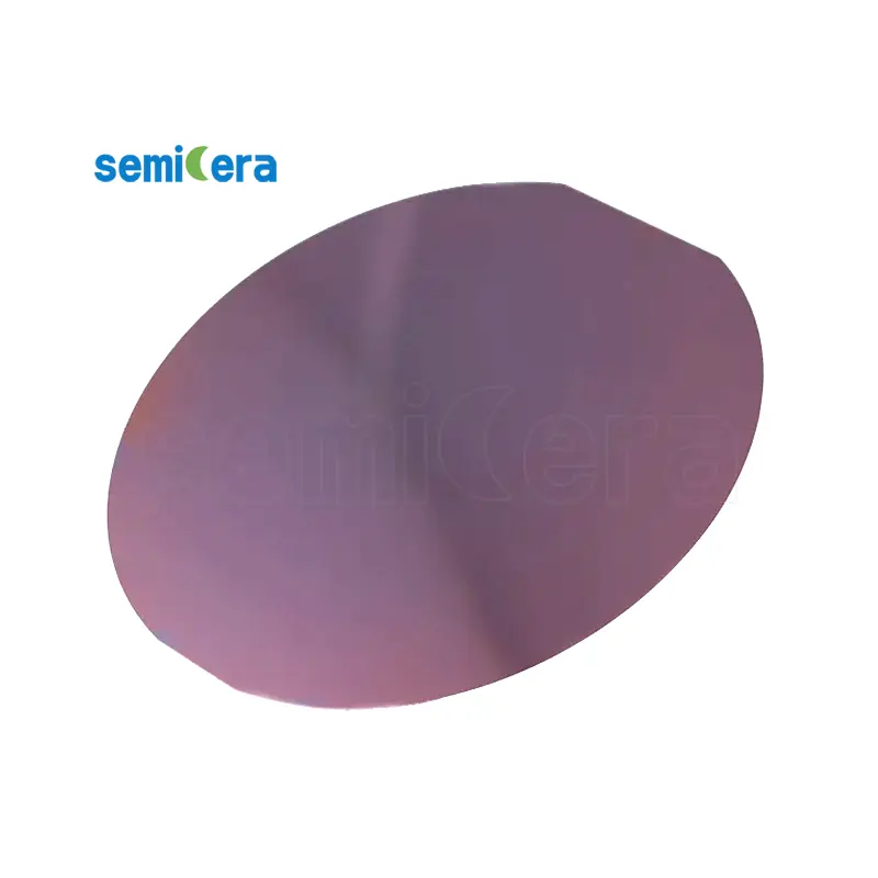
The Si Substrate by Semicera is an essential component in the production of high-performance semiconductor devices. Engineered from high-purity Silicon (Si), this substrate offers exceptional uniformity, stability, and excellent conductivity, making it ideal for a wide range of advanced applications in the semiconductor industry. Whether used in Si Wafer, SiC Substrate, SOI Wafer, or SiN Substrate production, the Semicera Si Substrate delivers consistent quality and superior performance to meet the growing demands of modern electronics and materials science.
Unmatched Performance with High Purity and Precision
Semicera’s Si Substrate is manufactured using advanced processes that ensure high purity and tight dimensional control. The substrate serves as the foundation for the production of a variety of high-performance materials, including Epi-Wafers and AlN Wafers. The precision and uniformity of the Si Substrate make it an excellent choice for creating thin-film epitaxial layers and other critical components used in the production of next-generation semiconductors. Whether you’re working with Gallium Oxide (Ga2O3) or other advanced materials, Semicera’s Si Substrate ensures the highest levels of reliability and performance.
Applications in Semiconductor Manufacturing
In the semiconductor industry, the Si Substrate from Semicera is utilized in a broad array of applications, including Si Wafer and SiC Substrate production, where it provides a stable, reliable base for the deposition of active layers. The substrate plays a critical role in fabricating SOI Wafers (Silicon On Insulator), which are essential for advanced microelectronics and integrated circuits. Furthermore, Epi-Wafers (epitaxial wafers) built on Si Substrates are integral in producing high-performance semiconductor devices such as power transistors, diodes, and integrated circuits.
The Si Substrate also supports the manufacturing of devices using Gallium Oxide (Ga2O3), a promising wide-bandgap material used for high-power applications in power electronics. Additionally, the compatibility of Semicera’s Si Substrate with AlN Wafers and other advanced substrates ensures that it can meet the diverse requirements of high-tech industries, making it an ideal solution for the production of cutting-edge devices in telecommunications, automotive, and industrial sectors.
Reliable and Consistent Quality for High-Tech Applications
The Si Substrate by Semicera is carefully engineered to meet the rigorous demands of semiconductor fabrication. Its exceptional structural integrity and high-quality surface properties make it the ideal material for use in cassette systems for wafer transport, as well as for creating high-precision layers in semiconductor devices. The substrate’s ability to maintain consistent quality under varying process conditions ensures minimal defects, enhancing the yield and performance of the final product.
With its superior thermal conductivity, mechanical strength, and high purity, Semicera’s Si Substrate is the material of choice for manufacturers looking to achieve the highest standards of precision, reliability, and performance in semiconductor production.
Choose Semicera’s Si Substrate for High-Purity, High-Performance Solutions
For manufacturers in the semiconductor industry, the Si Substrate from Semicera offers a robust, high-quality solution for a wide range of applications, from Si Wafer production to the creation of Epi-Wafers and SOI Wafers. With unmatched purity, precision, and reliability, this substrate enables the production of cutting-edge semiconductor devices, ensuring long-term performance and optimal efficiency. Choose Semicera for your Si substrate needs, and trust in a product designed to meet the demands of tomorrow’s technologies.
|
أغراض |
إنتاج |
بحث |
دمية |
|
المعلمات البلورية |
|||
|
polytype |
4H |
||
|
خطأ في اتجاه السطح |
4±0.15° |
||
|
المعلمات الكهربائية |
|||
|
Dopant |
نيتروجين من النوع |
||
|
المقاومة |
0.015-0.025OHM · سم |
||
|
المعلمات الميكانيكية |
|||
|
قطر |
150.0 ± 0.2mm |
||
|
سماكة |
350 ± 25 ميكرون |
||
|
الاتجاه المسطح الأولي |
[1-100]±5° |
||
|
طول مسطح أساسي |
47.5 ± 1.5mm |
||
|
شقة ثانوية |
لا أحد |
||
|
TTV |
≤5 ميكرون |
≤10 ميكرون |
≤15 ميكرون |
|
LTV |
≤3 ميكرون (5 ملم*5 ملم) |
≤5 ميكرون (5 ملم*5 ملم) |
≤10 ميكرون (5 ملم*5 ملم) |
|
قَوس |
-15μm ~ 15μm |
-35μm ~ 35μm |
-45μm ~ 45μm |
|
الاعوجاج |
≤35 ميكرون |
≤45 ميكرون |
≤55 ميكرون |
|
الخشونة الأمامية (si-face) (AFM) |
Ra≤0.2nm (5μm*5μm) |
||
|
بناء |
|||
|
كثافة micropipe |
<1 EA/CM2 |
<10 EA/CM2 |
<15 EA/CM2 |
|
الشوائب المعدنية |
≤5E10atoms/cm2 |
نا |
|
|
BPD |
≤1500 EA/CM2 |
≤3000 EA/CM2 |
نا |
|
TSD |
≤500 EA/CM2 |
≤1000 EA/CM2 |
نا |
|
الجودة الأمامية |
|||
|
أمام |
سي |
||
|
الانتهاء من السطح |
Si-Face CMP |
||
|
الجزيئات |
≤60A/WEFR (SIZE 30.3μM) |
نا |
|
|
الخدوش |
≤5ea/مم. الطول التراكمي ≤Diameter |
الطول التراكمي ≤2*القطر |
نا |
|
قشر البرتقال/الحفر/البقع/الدماغ/الشقوق/التلوث |
لا أحد |
نا |
|
|
رقائق الحافة/المسافات البادئة/الكسر/الألواح السداسية |
لا أحد |
||
|
المناطق polytype |
لا أحد |
منطقة تراكمية 20% |
التراكمية منطقة ≤30% |
|
وضع علامة ليزر الأمامية |
لا أحد |
||
|
جودة الظهر |
|||
|
الانتهاء من الظهر |
C-Face CMP |
||
|
الخدوش |
≤5EA/MM ، الطول التراكمي ≤2*القطر |
نا |
|
|
عيوب الظهر (رقائق الحافة/المسافات البادئة) |
لا أحد |
||
|
خشونة الظهر |
Ra≤0.2nm (5μm*5μm) |
||
|
عودة ليزر العلامات |
1 مم (من الحافة العليا) |
||
|
حافة |
|||
|
حافة |
شامفر |
||
|
التغليف |
|||
|
التغليف |
جاهز لـ EPI مع تغليف فراغ عبوات الكاسيت متعددة الفرس |
||
|
*الملاحظات : "NA" تعني عدم وجود عناصر طلب لم يتم ذكرها قد تشير إلى Semi. |
|||