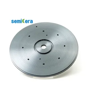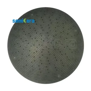
Silicon on Insulator Wafers from Semicera are designed to meet the growing demand for high-performance semiconductor solutions. Our SOI wafers offer superior electrical performance and reduced parasitic device capacitance, making them ideal for advanced applications such as MEMS devices, sensors, and integrated circuits. Semicera’s expertise in wafer production ensures that each SOI wafer provides reliable, high-quality results for your next-generation technology needs.
Our Silicon on Insulator Wafers offer an optimal balance between cost-effectiveness and performance. With soi wafer cost becoming increasingly competitive, these wafers are widely used in a range of industries, including microelectronics and optoelectronics. Semicera’s high-precision production process guarantees superior wafer bonding and uniformity, making them suitable for a variety of applications, from cavity SOI wafers to standard silicon wafers.
الميزات الرئيسية:
• High-quality SOI wafers optimized for performance in MEMS and other applications.
• Competitive soi wafer cost for businesses seeking advanced solutions without compromising quality.
• Ideal for cutting-edge technologies, offering enhanced electrical isolation and efficiency in silicon on insulator systems.
Our Silicon on Insulator Wafers are engineered to provide high-performance solutions, supporting the next wave of innovation in semiconductor technology. Whether you’re working on cavity SOI wafers, MEMS devices, or silicon on insulator components, Semicera delivers wafers that meet the highest standards in the industry.
|
أغراض |
إنتاج |
بحث |
دمية |
|
المعلمات البلورية |
|||
|
polytype |
4H |
||
|
خطأ في اتجاه السطح |
<11-20 >4±0.15° |
||
|
المعلمات الكهربائية |
|||
|
Dopant |
نيتروجين من النوع |
||
|
المقاومة |
0.015-0.025ohm·cm |
||
|
المعلمات الميكانيكية |
|||
|
قطر |
150.0±0.2mm |
||
|
سماكة |
350±25 μm |
||
|
الاتجاه المسطح الأولي |
[1-100]±5° |
||
|
طول مسطح أساسي |
47.5±1.5mm |
||
|
شقة ثانوية |
لا أحد |
||
|
TTV |
≤5 μm |
≤10 μm |
≤15 μm |
|
LTV |
≤3 μm(5mm*5mm) |
≤5 μm(5mm*5mm) |
≤10 μm(5mm*5mm) |
|
قَوس |
-15μm ~ 15μm |
-35μm ~ 35μm |
-45μm ~ 45μm |
|
الاعوجاج |
≤35 μm |
≤45 μm |
≤55 μm |
|
الخشونة الأمامية (si-face) (AFM) |
Ra≤0.2nm (5μm*5μm) |
||
|
بناء |
|||
|
كثافة micropipe |
<1 EA/CM2 |
<10 EA/CM2 |
<15 EA/CM2 |
|
الشوائب المعدنية |
≤5E10atoms/cm2 |
نا |
|
|
BPD |
≤1500 ea/cm2 |
≤3000 ea/cm2 |
نا |
|
TSD |
≤500 ea/cm2 |
≤1000 ea/cm2 |
نا |
|
الجودة الأمامية |
|||
|
أمام |
سي |
||
|
الانتهاء من السطح |
Si-Face CMP |
||
|
الجزيئات |
≤60ea/wafer (size≥0.3μm) |
نا |
|
|
الخدوش |
≤5ea/mm. Cumulative length ≤Diameter |
Cumulative length≤2*Diameter |
نا |
|
قشر البرتقال/الحفر/البقع/الدماغ/الشقوق/التلوث |
لا أحد |
نا |
|
|
رقائق الحافة/المسافات البادئة/الكسر/الألواح السداسية |
لا أحد |
||
|
المناطق polytype |
لا أحد |
Cumulative area≤20% |
Cumulative area≤30% |
|
وضع علامة ليزر الأمامية |
لا أحد |
||
|
جودة الظهر |
|||
|
الانتهاء من الظهر |
C-Face CMP |
||
|
الخدوش |
≤5ea/mm,Cumulative length≤2*Diameter |
نا |
|
|
عيوب الظهر (رقائق الحافة/المسافات البادئة) |
لا أحد |
||
|
خشونة الظهر |
Ra≤0.2nm (5μm*5μm) |
||
|
عودة ليزر العلامات |
1 مم (من الحافة العليا) |
||
|
حافة |
|||
|
حافة |
شامفر |
||
|
التغليف |
|||
|
التغليف |
جاهز لـ EPI مع تغليف فراغ عبوات الكاسيت متعددة الفرس |
||
|
*Notes: “NA” means no request Items not mentioned may refer to SEMI-STD. |
|||