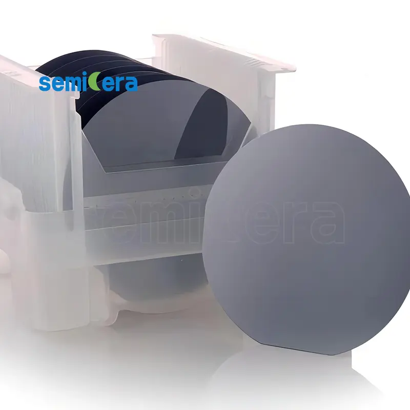
Semicera Silicon Substrates are crafted to meet the rigorous demands of the semiconductor industry, offering unparalleled quality and precision. These substrates provide a reliable foundation for various applications, from integrated circuits to photovoltaic cells, ensuring optimal performance and longevity.
The high purity of Semicera Silicon Substrates ensures minimal defects and superior electrical characteristics, which are critical for the production of high-efficiency electronic components. This level of purity helps in reducing energy loss and improving the overall efficiency of semiconductor devices.
Semicera employs state-of-the-art manufacturing techniques to produce silicon substrates with exceptional uniformity and flatness. This precision is essential for achieving consistent results in semiconductor fabrication, where even the slightest variation can impact device performance and yield.
Available in a variety of sizes and specifications, Semicera Silicon Substrates cater to a wide range of industrial needs. Whether you are developing cutting-edge microprocessors or solar panels, these substrates provide the flexibility and reliability required for your specific application.
Semicera is dedicated to supporting innovation and efficiency in the semiconductor industry. By providing high-quality silicon substrates, we enable manufacturers to push the boundaries of technology, delivering products that meet the evolving demands of the market. Trust Semicera for your next-generation electronic and photovoltaic solutions.
|
أغراض |
إنتاج |
بحث |
دمية |
|
المعلمات البلورية |
|||
|
polytype |
4H |
||
|
خطأ في اتجاه السطح |
4±0.15° |
||
|
المعلمات الكهربائية |
|||
|
Dopant |
نيتروجين من النوع |
||
|
المقاومة |
0.015-0.025OHM · سم |
||
|
المعلمات الميكانيكية |
|||
|
قطر |
150.0 ± 0.2mm |
||
|
سماكة |
350 ± 25 ميكرون |
||
|
الاتجاه المسطح الأولي |
[1-100]±5° |
||
|
طول مسطح أساسي |
47.5 ± 1.5mm |
||
|
شقة ثانوية |
لا أحد |
||
|
TTV |
≤5 ميكرون |
≤10 ميكرون |
≤15 ميكرون |
|
LTV |
≤3 ميكرون (5 ملم*5 ملم) |
≤5 ميكرون (5 ملم*5 ملم) |
≤10 ميكرون (5 ملم*5 ملم) |
|
قَوس |
-15μm ~ 15μm |
-35μm ~ 35μm |
-45μm ~ 45μm |
|
الاعوجاج |
≤35 ميكرون |
≤45 ميكرون |
≤55 ميكرون |
|
الخشونة الأمامية (si-face) (AFM) |
Ra≤0.2nm (5μm*5μm) |
||
|
بناء |
|||
|
كثافة micropipe |
<1 EA/CM2 |
<10 EA/CM2 |
<15 EA/CM2 |
|
الشوائب المعدنية |
≤5E10atoms/cm2 |
نا |
|
|
BPD |
≤1500 EA/CM2 |
≤3000 EA/CM2 |
نا |
|
TSD |
≤500 EA/CM2 |
≤1000 EA/CM2 |
نا |
|
الجودة الأمامية |
|||
|
أمام |
سي |
||
|
الانتهاء من السطح |
Si-Face CMP |
||
|
الجزيئات |
≤60A/WEFR (SIZE 30.3μM) |
نا |
|
|
الخدوش |
≤5ea/مم. الطول التراكمي ≤Diameter |
الطول التراكمي ≤2*القطر |
نا |
|
قشر البرتقال/الحفر/البقع/الدماغ/الشقوق/التلوث |
لا أحد |
نا |
|
|
رقائق الحافة/المسافات البادئة/الكسر/الألواح السداسية |
لا أحد |
||
|
المناطق polytype |
لا أحد |
منطقة تراكمية 20% |
التراكمية منطقة ≤30% |
|
وضع علامة ليزر الأمامية |
لا أحد |
||
|
جودة الظهر |
|||
|
الانتهاء من الظهر |
C-Face CMP |
||
|
الخدوش |
≤5EA/MM ، الطول التراكمي ≤2*القطر |
نا |
|
|
عيوب الظهر (رقائق الحافة/المسافات البادئة) |
لا أحد |
||
|
خشونة الظهر |
Ra≤0.2nm (5μm*5μm) |
||
|
عودة ليزر العلامات |
1 مم (من الحافة العليا) |
||
|
حافة |
|||
|
حافة |
شامفر |
||
|
التغليف |
|||
|
التغليف |
جاهز لـ EPI مع تغليف فراغ عبوات الكاسيت متعددة الفرس |
||
|
*الملاحظات : "NA" تعني عدم وجود عناصر طلب لم يتم ذكرها قد تشير إلى Semi. |
|||


