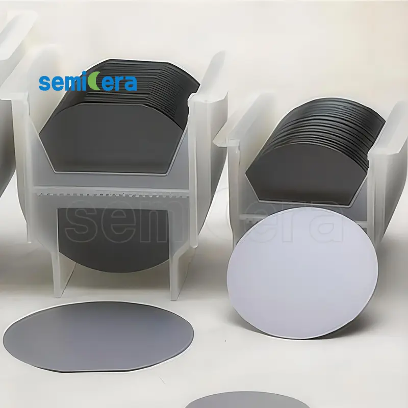
Semicera Silicon Wafers are meticulously crafted to serve as the foundation for a wide array of semiconductor devices, from microprocessors to photovoltaic cells. These wafers are engineered with high precision and purity, ensuring optimal performance in various electronic applications.
Manufactured using advanced techniques, Semicera Silicon Wafers exhibit exceptional flatness and uniformity, which are crucial for achieving high yields in semiconductor fabrication. This level of precision helps in minimizing defects and improving the overall efficiency of electronic components.
The superior quality of Semicera Silicon Wafers is evident in their electrical characteristics, which contribute to the enhanced performance of semiconductor devices. With low impurity levels and high crystal quality, these wafers provide the ideal platform for developing high-performance electronics.
Available in various sizes and specifications, Semicera Silicon Wafers can be tailored to meet the specific needs of different industries, including computing, telecommunications, and renewable energy. Whether for large-scale manufacturing or specialized research, these wafers deliver reliable results.
Semicera is committed to supporting the growth and innovation of the semiconductor industry by providing high-quality silicon wafers that meet the highest industry standards. With a focus on precision and reliability, Semicera enables manufacturers to push the boundaries of technology, ensuring their products stay at the forefront of the market.
|
أغراض |
إنتاج |
بحث |
دمية |
|
المعلمات البلورية |
|||
|
polytype |
4H |
||
|
خطأ في اتجاه السطح |
4±0.15° |
||
|
المعلمات الكهربائية |
|||
|
Dopant |
نيتروجين من النوع |
||
|
المقاومة |
0.015-0.025OHM · سم |
||
|
المعلمات الميكانيكية |
|||
|
قطر |
150.0 ± 0.2mm |
||
|
سماكة |
350 ± 25 ميكرون |
||
|
الاتجاه المسطح الأولي |
[1-100]±5° |
||
|
طول مسطح أساسي |
47.5 ± 1.5mm |
||
|
شقة ثانوية |
لا أحد |
||
|
TTV |
≤5 ميكرون |
≤10 ميكرون |
≤15 ميكرون |
|
LTV |
≤3 ميكرون (5 ملم*5 ملم) |
≤5 ميكرون (5 ملم*5 ملم) |
≤10 ميكرون (5 ملم*5 ملم) |
|
قَوس |
-15μm ~ 15μm |
-35μm ~ 35μm |
-45μm ~ 45μm |
|
الاعوجاج |
≤35 ميكرون |
≤45 ميكرون |
≤55 ميكرون |
|
الخشونة الأمامية (si-face) (AFM) |
Ra≤0.2nm (5μm*5μm) |
||
|
بناء |
|||
|
كثافة micropipe |
<1 EA/CM2 |
<10 EA/CM2 |
<15 EA/CM2 |
|
الشوائب المعدنية |
≤5E10atoms/cm2 |
نا |
|
|
BPD |
≤1500 EA/CM2 |
≤3000 EA/CM2 |
نا |
|
TSD |
≤500 EA/CM2 |
≤1000 EA/CM2 |
نا |
|
الجودة الأمامية |
|||
|
أمام |
سي |
||
|
الانتهاء من السطح |
Si-Face CMP |
||
|
الجزيئات |
≤60A/WEFR (SIZE 30.3μM) |
نا |
|
|
الخدوش |
≤5ea/مم. الطول التراكمي ≤Diameter |
الطول التراكمي ≤2*القطر |
نا |
|
قشر البرتقال/الحفر/البقع/الدماغ/الشقوق/التلوث |
لا أحد |
نا |
|
|
رقائق الحافة/المسافات البادئة/الكسر/الألواح السداسية |
لا أحد |
||
|
المناطق polytype |
لا أحد |
منطقة تراكمية 20% |
التراكمية منطقة ≤30% |
|
وضع علامة ليزر الأمامية |
لا أحد |
||
|
جودة الظهر |
|||
|
الانتهاء من الظهر |
C-Face CMP |
||
|
الخدوش |
≤5EA/MM ، الطول التراكمي ≤2*القطر |
نا |
|
|
عيوب الظهر (رقائق الحافة/المسافات البادئة) |
لا أحد |
||
|
خشونة الظهر |
Ra≤0.2nm (5μm*5μm) |
||
|
عودة ليزر العلامات |
1 مم (من الحافة العليا) |
||
|
حافة |
|||
|
حافة |
شامفر |
||
|
التغليف |
|||
|
التغليف |
جاهز لـ EPI مع تغليف فراغ عبوات الكاسيت متعددة الفرس |
||
|
*الملاحظات : "NA" تعني عدم وجود عناصر طلب لم يتم ذكرها قد تشير إلى Semi. |
|||


