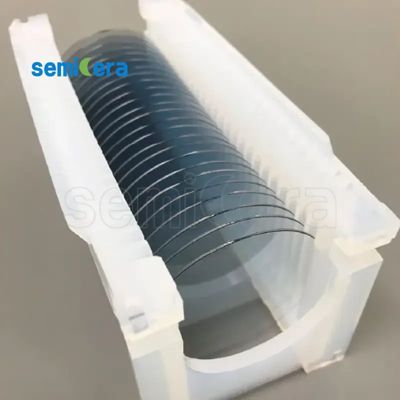
Semicera is proud to present the Ga2O3 Substrate, a cutting-edge material poised to revolutionize power electronics and optoelectronics. Gallium Oxide (Ga2O3) substrates are known for their ultra-wide bandgap, making them ideal for high-power and high-frequency devices.
Schlüsselmerkmale:
• Ultra-Wide Bandgap: Ga2O3 offers a bandgap of approximately 4.8 eV, significantly enhancing its ability to handle high voltages and temperatures compared to traditional materials like Silicon and GaN.
• High Breakdown Voltage: With an exceptional breakdown field, the Ga2O3 Substrate is perfect for devices requiring high-voltage operation, ensuring greater efficiency and reliability.
• Thermal Stability: The material’s superior thermal stability makes it suitable for applications in extreme environments, maintaining performance even under harsh conditions.
• Versatile Applications: Ideal for use in high-efficiency power transistors, UV optoelectronic devices, and more, providing a robust foundation for advanced electronic systems.
Experience the future of semiconductor technology with Semicera’s Ga2O3 Substrate. Designed to meet the growing demands of high-power and high-frequency electronics, this substrate sets a new standard for performance and durability. Trust Semicera to deliver innovative solutions for your most challenging applications.
|
Artikel |
Produktion |
Forschung |
Dummy |
|
Kristallparameter |
|||
|
Polytype |
4H |
||
|
Oberflächenorientierungsfehler |
4±0.15° |
||
|
Elektrische Parameter |
|||
|
Dopant |
Stickstoff vom Typ N |
||
|
Widerstand |
0,015-0.025OHM · cm |
||
|
Mechanische Parameter |
|||
|
Durchmesser |
150,0 ± 0,2 mm |
||
|
Dicke |
350 ± 25 µm |
||
|
Primäre flache Orientierung |
[1-100]±5° |
||
|
Primäre flache Länge |
47,5 ± 1,5 mm |
||
|
Sekundäre flache |
Keiner |
||
|
Ttv |
≤5 µm |
≤10 µm |
≤15 µm |
|
LTV |
≤3 μm (5 mm*5 mm) |
≤5 μm (5 mm*5 mm) |
≤10 μm (5 mm*5 mm) |
|
Bogen |
-15 μm ~ 15 μm |
-35 μm ~ 35 μm |
-45 μm ~ 45 μm |
|
Kette |
≤35 µm |
≤45 µm |
≤55 µm |
|
Front (Si-Face) Rauheit (AFM) |
Ra ≤ 0,2 nm (5 & mgr; m*5 μm) |
||
|
Struktur |
|||
|
Mikropipe -Dichte |
<1 EA/CM2 |
<10 EA/CM2 |
<15 EA/CM2 |
|
Metallverunreinigungen |
≤5E10atoms/cm2 |
N / A |
|
|
BPD |
≤1500 EA/CM2 |
≤3000 EA/CM2 |
N / A |
|
TSD |
≤500 EA/CM2 |
≤1000 EA/CM2 |
N / A |
|
Frontqualität |
|||
|
Front |
Si |
||
|
Oberflächenbeschaffung |
Si-Face CMP |
||
|
Partikel |
≤60ea/Wafer (Größe ≥ 0,3 μm) |
N / A |
|
|
Kratzer |
≤5ea/mm. Kumulative Länge ≤ Diameter |
Kumulative Länge ≤ 2*Durchmesser |
N / A |
|
Orangenschale/Pits/Flecken/Streifen/Risse/Kontamination |
Keiner |
N / A |
|
|
Kantenchips/Eingeweide/Fraktur-/Sechskantplatten |
Keiner |
||
|
Polytyperbereiche |
Keiner |
Kumulative Fläche ≤ 2010TP3T |
Kumulative Fläche ≤ 30% |
|
Frontlasermarkierung |
Keiner |
||
|
Rückenqualität |
|||
|
Rückbeschluss |
C-Face CMP |
||
|
Kratzer |
≤5ea/mm, kumulative Länge ≤ 2*Durchmesser |
N / A |
|
|
Rückenfehler (Kantenchips/Eingebiete) |
Keiner |
||
|
Rückenrauheit |
Ra ≤ 0,2 nm (5 & mgr; m*5 μm) |
||
|
Rückmarkierung von Laser |
1 mm (von der Oberkante) |
||
|
Rand |
|||
|
Rand |
Chamfer |
||
|
Packaging |
|||
|
Packaging |
Epi-ready with vacuum packaging Multi-wafer cassette packaging |
||
|
*Notes: “NA” means no request Items not mentioned may refer to SEMI-STD. |
|||


