Semizelle introduces its high-quality Si -Epitaxie services, designed to meet the exacting standards of today’s semiconductor industry. Epitaxial silicon layers are critical for the performance and reliability of electronic devices, and our Si Epitaxy solutions ensure that your components achieve optimal functionality.
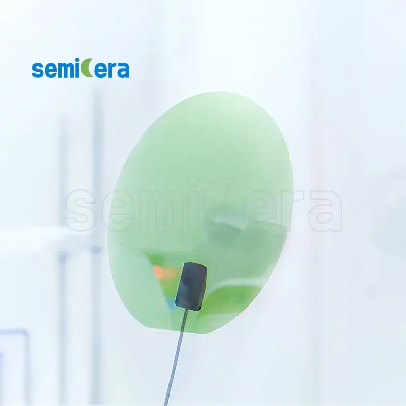
Precision-Grown Silicon Layers Semizelle understands that the foundation of high-performance devices lies in the quality of the materials used. Our Si -Epitaxie process is meticulously controlled to produce silicon layers with exceptional uniformity and crystal integrity. These layers are essential for applications ranging from microelectronics to advanced power devices, where consistency and reliability are paramount.
Optimized for Device Performance Der Si -Epitaxie services offered by Semicera are tailored to enhance the electrical properties of your devices. By growing high-purity silicon layers with low defect densities, we ensure that your components perform at their best, with improved carrier mobility and minimized electrical resistivity. This optimization is critical for achieving the high-speed and high-efficiency characteristics demanded by modern technology.
Versatility in Applications Semizelle’s Si -Epitaxie is suitable for a wide range of applications, including the production of CMOS transistors, power MOSFETs, and bipolar junction transistors. Our flexible process allows for customization based on the specific requirements of your project, whether you need thin layers for high-frequency applications or thicker layers for power devices.
Superior Material Quality Quality is at the heart of everything we do at Semicera. Our Si -Epitaxie process uses state-of-the-art equipment and techniques to ensure that each silicon layer meets the highest standards of purity and structural integrity. This attention to detail minimizes the occurrence of defects that could impact device performance, resulting in more reliable and longer-lasting components.
Commitment to Innovation Semizelle is committed to staying at the forefront of semiconductor technology. Our Si -Epitaxie services reflect this commitment, incorporating the latest advancements in epitaxial growth techniques. We continuously refine our processes to deliver silicon layers that meet the evolving needs of the industry, ensuring that your products remain competitive in the market.
Tailored Solutions for Your Needs Understanding that every project is unique, Semizelle offers customized Si -Epitaxie solutions to match your specific needs. Whether you require particular doping profiles, layer thicknesses, or surface finishes, our team works closely with you to deliver a product that meets your precise specifications.
|
Artikel |
Produktion |
Forschung |
Dummy |
|
Kristallparameter |
|||
|
Polytype |
4H |
||
|
Oberflächenorientierungsfehler |
4±0.15° |
||
|
Elektrische Parameter |
|||
|
Dopant |
Stickstoff vom Typ N |
||
|
Widerstand |
0,015-0.025OHM · cm |
||
|
Mechanische Parameter |
|||
|
Durchmesser |
150,0 ± 0,2 mm |
||
|
Dicke |
350 ± 25 µm |
||
|
Primäre flache Orientierung |
[1-100]±5° |
||
|
Primäre flache Länge |
47,5 ± 1,5 mm |
||
|
Sekundäre flache |
Keiner |
||
|
Ttv |
≤5 µm |
≤10 µm |
≤15 µm |
|
LTV |
≤3 μm (5 mm*5 mm) |
≤5 μm (5 mm*5 mm) |
≤10 μm (5 mm*5 mm) |
|
Bogen |
-15 μm ~ 15 μm |
-35 μm ~ 35 μm |
-45 μm ~ 45 μm |
|
Kette |
≤35 µm |
≤45 µm |
≤55 µm |
|
Front (Si-Face) Rauheit (AFM) |
Ra ≤ 0,2 nm (5 & mgr; m*5 μm) |
||
|
Struktur |
|||
|
Mikropipe -Dichte |
<1 EA/CM2 |
<10 EA/CM2 |
<15 EA/CM2 |
|
Metallverunreinigungen |
≤5E10atoms/cm2 |
N / A |
|
|
BPD |
≤1500 EA/CM2 |
≤3000 EA/CM2 |
N / A |
|
TSD |
≤500 EA/CM2 |
≤1000 EA/CM2 |
N / A |
|
Frontqualität |
|||
|
Front |
Si |
||
|
Oberflächenbeschaffung |
Si-Face CMP |
||
|
Partikel |
≤60ea/Wafer (Größe ≥ 0,3 μm) |
N / A |
|
|
Kratzer |
≤5ea/mm. Kumulative Länge ≤ Diameter |
Kumulative Länge ≤ 2*Durchmesser |
N / A |
|
Orangenschale/Pits/Flecken/Streifen/Risse/Kontamination |
Keiner |
N / A |
|
|
Kantenchips/Eingeweide/Fraktur-/Sechskantplatten |
Keiner |
||
|
Polytyperbereiche |
Keiner |
Kumulative Fläche ≤ 2010TP3T |
Kumulative Fläche ≤ 30% |
|
Frontlasermarkierung |
Keiner |
||
|
Rückenqualität |
|||
|
Rückbeschluss |
C-Face CMP |
||
|
Kratzer |
≤5ea/mm, kumulative Länge ≤ 2*Durchmesser |
N / A |
|
|
Rückenfehler (Kantenchips/Eingebiete) |
Keiner |
||
|
Rückenrauheit |
Ra ≤ 0,2 nm (5 & mgr; m*5 μm) |
||
|
Rückmarkierung von Laser |
1 mm (von der Oberkante) |
||
|
Rand |
|||
|
Rand |
Chamfer |
||
|
Packaging |
|||
|
Packaging |
Epi-ready with vacuum packaging Multi-wafer cassette packaging |
||
|
*Notes: “NA” means no request Items not mentioned may refer to SEMI-STD. |
|||


