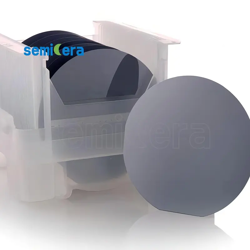
Semicera Silicon Substrates are crafted to meet the rigorous demands of the semiconductor industry, offering unparalleled quality and precision. These substrates provide a reliable foundation for various applications, from integrated circuits to photovoltaic cells, ensuring optimal performance and longevity.
The high purity of Semicera Silicon Substrates ensures minimal defects and superior electrical characteristics, which are critical for the production of high-efficiency electronic components. This level of purity helps in reducing energy loss and improving the overall efficiency of semiconductor devices.
Semicera employs state-of-the-art manufacturing techniques to produce silicon substrates with exceptional uniformity and flatness. This precision is essential for achieving consistent results in semiconductor fabrication, where even the slightest variation can impact device performance and yield.
Available in a variety of sizes and specifications, Semicera Silicon Substrates cater to a wide range of industrial needs. Whether you are developing cutting-edge microprocessors or solar panels, these substrates provide the flexibility and reliability required for your specific application.
Semicera is dedicated to supporting innovation and efficiency in the semiconductor industry. By providing high-quality silicon substrates, we enable manufacturers to push the boundaries of technology, delivering products that meet the evolving demands of the market. Trust Semicera for your next-generation electronic and photovoltaic solutions.
|
Artikel |
Produktion |
Forschung |
Dummy |
|
Kristallparameter |
|||
|
Polytype |
4H |
||
|
Oberflächenorientierungsfehler |
4±0.15° |
||
|
Elektrische Parameter |
|||
|
Dopant |
Stickstoff vom Typ N |
||
|
Widerstand |
0,015-0.025OHM · cm |
||
|
Mechanische Parameter |
|||
|
Durchmesser |
150,0 ± 0,2 mm |
||
|
Dicke |
350 ± 25 µm |
||
|
Primäre flache Orientierung |
[1-100]±5° |
||
|
Primäre flache Länge |
47,5 ± 1,5 mm |
||
|
Sekundäre flache |
Keiner |
||
|
Ttv |
≤5 µm |
≤10 µm |
≤15 µm |
|
LTV |
≤3 μm (5 mm*5 mm) |
≤5 μm (5 mm*5 mm) |
≤10 μm (5 mm*5 mm) |
|
Bogen |
-15 μm ~ 15 μm |
-35 μm ~ 35 μm |
-45 μm ~ 45 μm |
|
Kette |
≤35 µm |
≤45 µm |
≤55 µm |
|
Front (Si-Face) Rauheit (AFM) |
Ra ≤ 0,2 nm (5 & mgr; m*5 μm) |
||
|
Struktur |
|||
|
Mikropipe -Dichte |
<1 EA/CM2 |
<10 EA/CM2 |
<15 EA/CM2 |
|
Metallverunreinigungen |
≤5E10atoms/cm2 |
N / A |
|
|
BPD |
≤1500 EA/CM2 |
≤3000 EA/CM2 |
N / A |
|
TSD |
≤500 EA/CM2 |
≤1000 EA/CM2 |
N / A |
|
Frontqualität |
|||
|
Front |
Si |
||
|
Oberflächenbeschaffung |
Si-Face CMP |
||
|
Partikel |
≤60ea/Wafer (Größe ≥ 0,3 μm) |
N / A |
|
|
Kratzer |
≤5ea/mm. Kumulative Länge ≤ Diameter |
Kumulative Länge ≤ 2*Durchmesser |
N / A |
|
Orangenschale/Pits/Flecken/Streifen/Risse/Kontamination |
Keiner |
N / A |
|
|
Kantenchips/Eingeweide/Fraktur-/Sechskantplatten |
Keiner |
||
|
Polytyperbereiche |
Keiner |
Kumulative Fläche ≤ 2010TP3T |
Kumulative Fläche ≤ 30% |
|
Frontlasermarkierung |
Keiner |
||
|
Rückenqualität |
|||
|
Rückbeschluss |
C-Face CMP |
||
|
Kratzer |
≤5ea/mm, kumulative Länge ≤ 2*Durchmesser |
N / A |
|
|
Rückenfehler (Kantenchips/Eingebiete) |
Keiner |
||
|
Rückenrauheit |
Ra ≤ 0,2 nm (5 & mgr; m*5 μm) |
||
|
Rückmarkierung von Laser |
1 mm (von der Oberkante) |
||
|
Rand |
|||
|
Rand |
Chamfer |
||
|
Packaging |
|||
|
Packaging |
Epi-ready with vacuum packaging Multi-wafer cassette packaging |
||
|
*Notes: “NA” means no request Items not mentioned may refer to SEMI-STD. |
|||


