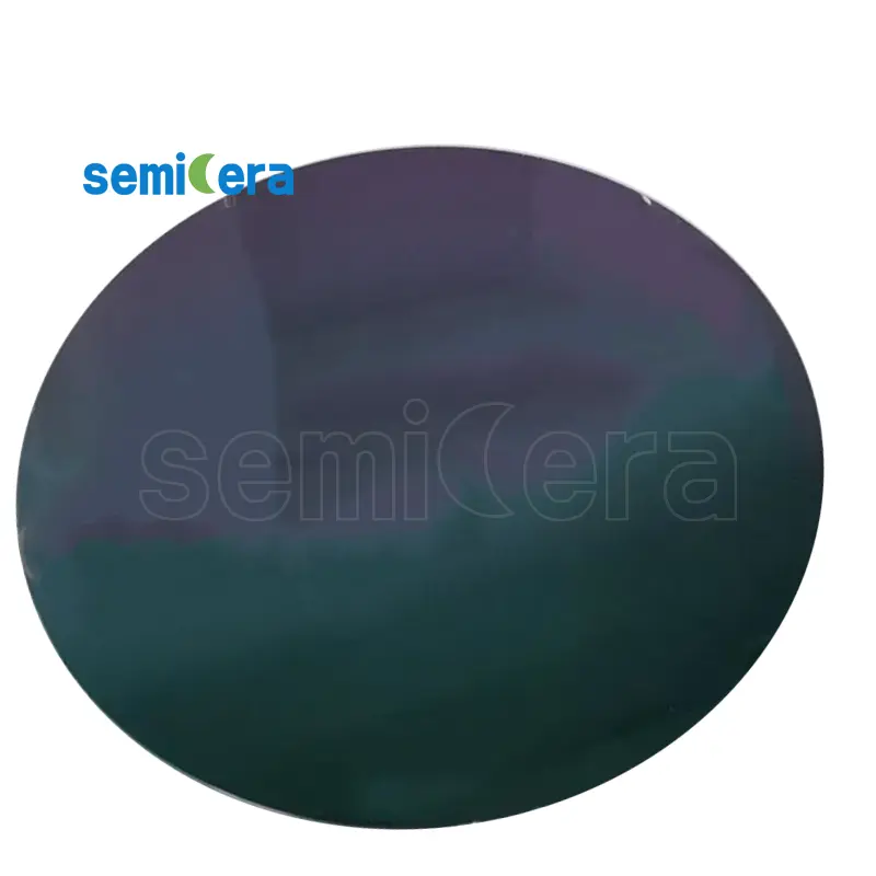
Semicera’s SOI Wafer (Silicon On Insulator) is designed to deliver superior electrical isolation and thermal performance. This innovative wafer structure, featuring a silicon layer on an insulating layer, ensures enhanced device performance and reduced power consumption, making it ideal for a variety of high-tech applications.
Our SOI wafers offer exceptional benefits for integrated circuits by minimizing parasitic capacitance and improving device speed and efficiency. This is crucial for modern electronics, where high performance and energy efficiency are essential for both consumer and industrial applications.
Semicera employs advanced manufacturing techniques to produce SOI wafers with consistent quality and reliability. These wafers provide excellent thermal insulation, making them suitable for use in environments where heat dissipation is a concern, such as in high-density electronic devices and power management systems.
The use of SOI wafers in semiconductor fabrication allows for the development of smaller, faster, and more reliable chips. Semicera’s commitment to precision engineering ensures that our SOI wafers meet the high standards required for cutting-edge technologies in fields like telecommunications, automotive, and consumer electronics.
Choosing Semicera’s SOI Wafer means investing in a product that supports the advancement of electronic and microelectronic technologies. Our wafers are designed to provide enhanced performance and durability, contributing to the success of your high-tech projects and ensuring that you stay at the forefront of innovation.
|
Artikel |
Produktion |
Forschung |
Dummy |
|
Kristallparameter |
|||
|
Polytype |
4H |
||
|
Oberflächenorientierungsfehler |
4±0.15° |
||
|
Elektrische Parameter |
|||
|
Dopant |
Stickstoff vom Typ N |
||
|
Widerstand |
0,015-0.025OHM · cm |
||
|
Mechanische Parameter |
|||
|
Durchmesser |
150,0 ± 0,2 mm |
||
|
Dicke |
350 ± 25 µm |
||
|
Primäre flache Orientierung |
[1-100]±5° |
||
|
Primäre flache Länge |
47,5 ± 1,5 mm |
||
|
Sekundäre flache |
Keiner |
||
|
Ttv |
≤5 µm |
≤10 µm |
≤15 µm |
|
LTV |
≤3 μm (5 mm*5 mm) |
≤5 μm (5 mm*5 mm) |
≤10 μm (5 mm*5 mm) |
|
Bogen |
-15 μm ~ 15 μm |
-35 μm ~ 35 μm |
-45 μm ~ 45 μm |
|
Kette |
≤35 µm |
≤45 µm |
≤55 µm |
|
Front (Si-Face) Rauheit (AFM) |
Ra ≤ 0,2 nm (5 & mgr; m*5 μm) |
||
|
Struktur |
|||
|
Mikropipe -Dichte |
<1 EA/CM2 |
<10 EA/CM2 |
<15 EA/CM2 |
|
Metallverunreinigungen |
≤5E10atoms/cm2 |
N / A |
|
|
BPD |
≤1500 EA/CM2 |
≤3000 EA/CM2 |
N / A |
|
TSD |
≤500 EA/CM2 |
≤1000 EA/CM2 |
N / A |
|
Frontqualität |
|||
|
Front |
Si |
||
|
Oberflächenbeschaffung |
Si-Face CMP |
||
|
Partikel |
≤60ea/Wafer (Größe ≥ 0,3 μm) |
N / A |
|
|
Kratzer |
≤5ea/mm. Kumulative Länge ≤ Diameter |
Kumulative Länge ≤ 2*Durchmesser |
N / A |
|
Orangenschale/Pits/Flecken/Streifen/Risse/Kontamination |
Keiner |
N / A |
|
|
Kantenchips/Eingeweide/Fraktur-/Sechskantplatten |
Keiner |
||
|
Polytyperbereiche |
Keiner |
Kumulative Fläche ≤ 2010TP3T |
Kumulative Fläche ≤ 30% |
|
Frontlasermarkierung |
Keiner |
||
|
Rückenqualität |
|||
|
Rückbeschluss |
C-Face CMP |
||
|
Kratzer |
≤5ea/mm, kumulative Länge ≤ 2*Durchmesser |
N / A |
|
|
Rückenfehler (Kantenchips/Eingebiete) |
Keiner |
||
|
Rückenrauheit |
Ra ≤ 0,2 nm (5 & mgr; m*5 μm) |
||
|
Rückmarkierung von Laser |
1 mm (von der Oberkante) |
||
|
Rand |
|||
|
Rand |
Chamfer |
||
|
Packaging |
|||
|
Packaging |
Epi-ready with vacuum packaging Multi-wafer cassette packaging |
||
|
*Notes: “NA” means no request Items not mentioned may refer to SEMI-STD. |
|||


