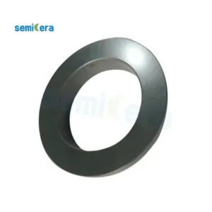
The Silicon Film by Semicera is a high-quality, precision-engineered material designed to meet the stringent requirements of the semiconductor industry. Manufactured from pure silicon, this thin-film solution offers excellent uniformity, high purity, and exceptional electrical and thermal properties. It is ideal for use in various semiconductor applications, including the production of Si Wafer, SiC Substrate, SOI Wafer, SiN Substrate, and Epi-Wafer. Semicera’s Silicon Film ensures reliable and consistent performance, making it an essential material for advanced microelectronics.
Superior Quality and Performance for Semiconductor Manufacturing
Semicera’s Silicon Film is known for its outstanding mechanical strength, high thermal stability, and low defect rates, all of which are crucial in the fabrication of high-performance semiconductors. Whether used in the production of Gallium Oxide (Ga2O3) devices, AlN Wafer, or Epi-Wafers, the film provides a strong foundation for thin-film deposition and epitaxial growth. Its compatibility with other semiconductor substrates like SiC Substrate and SOI Wafers ensures seamless integration into existing manufacturing processes, helping to maintain high yields and consistent product quality.
Anwendungen in der Halbleiterindustrie
In the semiconductor industry, Semicera’s Silicon Film is utilized in a wide range of applications, from the production of Si Wafer and SOI Wafer to more specialized uses like SiN Substrate and Epi-Wafer creation. The high purity and precision of this film make it essential in the production of advanced components used in everything from microprocessors and integrated circuits to optoelectronic devices.
The Silicon Film plays a critical role in semiconductor processes such as epitaxial growth, wafer bonding, and thin-film deposition. Its reliable properties are especially valuable for industries that require highly controlled environments, such as cleanrooms in semiconductor fabs. Additionally, the Silicon Film can be integrated into cassette systems for efficient wafer handling and transport during production.
Long-Term Reliability and Consistency
One of the key benefits of using Semicera’s Silicon Film is its long-term reliability. With its excellent durability and consistent quality, this film provides a dependable solution for high-volume production environments. Whether it’s used in high-precision semiconductor devices or advanced electronic applications, Semicera’s Silicon Film ensures that manufacturers can achieve high performance and reliability across a wide range of products.
Why Choose Semicera’s Silicon Film?
The Silicon Film from Semicera is an essential material for cutting-edge applications in the semiconductor industry. Its high-performance properties, including excellent thermal stability, high purity, and mechanical strength, make it the ideal choice for manufacturers looking to achieve the highest standards in semiconductor production. From Si Wafer and SiC Substrate to the production of Gallium Oxide Ga2O3 devices, this film delivers unmatched quality and performance.
With Semicera’s Silicon Film, you can trust in a product that meets the needs of modern semiconductor manufacturing, providing a reliable foundation for the next generation of electronics.
|
Artikel |
Produktion |
Forschung |
Dummy |
|
Kristallparameter |
|||
|
Polytype |
4H |
||
|
Oberflächenorientierungsfehler |
4±0.15° |
||
|
Elektrische Parameter |
|||
|
Dopant |
Stickstoff vom Typ N |
||
|
Widerstand |
0,015-0.025OHM · cm |
||
|
Mechanische Parameter |
|||
|
Durchmesser |
150,0 ± 0,2 mm |
||
|
Dicke |
350 ± 25 µm |
||
|
Primäre flache Orientierung |
[1-100]±5° |
||
|
Primäre flache Länge |
47,5 ± 1,5 mm |
||
|
Sekundäre flache |
Keiner |
||
|
Ttv |
≤5 µm |
≤10 µm |
≤15 µm |
|
LTV |
≤3 μm (5 mm*5 mm) |
≤5 μm (5 mm*5 mm) |
≤10 μm (5 mm*5 mm) |
|
Bogen |
-15 μm ~ 15 μm |
-35 μm ~ 35 μm |
-45 μm ~ 45 μm |
|
Kette |
≤35 µm |
≤45 µm |
≤55 µm |
|
Front (Si-Face) Rauheit (AFM) |
Ra ≤ 0,2 nm (5 & mgr; m*5 μm) |
||
|
Struktur |
|||
|
Mikropipe -Dichte |
<1 EA/CM2 |
<10 EA/CM2 |
<15 EA/CM2 |
|
Metallverunreinigungen |
≤5E10atoms/cm2 |
N / A |
|
|
BPD |
≤1500 EA/CM2 |
≤3000 EA/CM2 |
N / A |
|
TSD |
≤500 EA/CM2 |
≤1000 EA/CM2 |
N / A |
|
Frontqualität |
|||
|
Front |
Si |
||
|
Oberflächenbeschaffung |
Si-Face CMP |
||
|
Partikel |
≤60ea/Wafer (Größe ≥ 0,3 μm) |
N / A |
|
|
Kratzer |
≤5ea/mm. Kumulative Länge ≤ Diameter |
Kumulative Länge ≤ 2*Durchmesser |
N / A |
|
Orangenschale/Pits/Flecken/Streifen/Risse/Kontamination |
Keiner |
N / A |
|
|
Kantenchips/Eingeweide/Fraktur-/Sechskantplatten |
Keiner |
||
|
Polytyperbereiche |
Keiner |
Kumulative Fläche ≤ 2010TP3T |
Kumulative Fläche ≤ 30% |
|
Frontlasermarkierung |
Keiner |
||
|
Rückenqualität |
|||
|
Rückbeschluss |
C-Face CMP |
||
|
Kratzer |
≤5ea/mm, kumulative Länge ≤ 2*Durchmesser |
N / A |
|
|
Rückenfehler (Kantenchips/Eingebiete) |
Keiner |
||
|
Rückenrauheit |
Ra ≤ 0,2 nm (5 & mgr; m*5 μm) |
||
|
Rückmarkierung von Laser |
1 mm (von der Oberkante) |
||
|
Rand |
|||
|
Rand |
Chamfer |
||
|
Packaging |
|||
|
Packaging |
Epi-ready with vacuum packaging Multi-wafer cassette packaging |
||
|
*Notes: “NA” means no request Items not mentioned may refer to SEMI-STD. |
|||