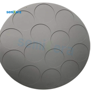
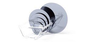
An epitaxial silicon wafer is a specialized type of silicon wafer featuring a thin, high-quality crystalline layer known as the epitaxial layer, which is grown on its surface. This epitaxial layer is engineered to enhance the electrical properties of the wafer. You’ll often find these epitaxial wafers in advanced semiconductor devices, where precision and performance are crucial. By utilizing an epi wafer, manufacturers can produce microchips and power devices that operate faster, consume less energy, and handle higher voltages. These epitaxial silicon wafers play a key role in the electronics you rely on every day, from smartphones to electric vehicles.
Key Takeaways
- Epitaxial silicon wafers have a smooth crystal layer. This improves how electricity flows, making them key for modern electronics.
- These wafers can be adjusted by adding materials. This helps makers design them for things like microchips and power tools.
- Careful checks are needed to make sure these wafers work well. They must meet tough rules to handle hard tasks.
- Epitaxial silicon wafers help make gadgets smaller and stronger. This is why we have tiny phones and electric cars.
- Using epitaxial silicon wafers helps create new ideas. They are important for green energy, car tech, and future tools like quantum computers.
What Is an Epitaxial Silicon Wafer?

Definition and Basic Concept
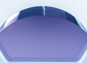
An epitaxial silicon wafer is a type of silicon wafer that has a thin, high-quality crystalline layer grown on its surface. This layer, called the epitaxial layer, is carefully engineered to have specific electrical properties. You can think of it as a customized coating that enhances the wafer’s performance. The term “epitaxial” comes from the Greek words “epi,” meaning “upon,” and “taxis,” meaning “arrangement.” It refers to how the new layer aligns perfectly with the crystal structure of the base wafer.
This alignment is crucial. It ensures that the epitaxial layer has fewer defects, which improves the wafer’s ability to conduct electricity. Manufacturers use this process to create wafers that meet the demanding requirements of modern electronics. Without this precise engineering, many advanced devices would not function as efficiently.
Key Properties of Epitaxial Layers
The epitaxial layer has several unique properties that make it valuable in semiconductor manufacturing. First, it offers excellent electrical conductivity. This allows devices to operate faster and more reliably. Second, the layer can be tailored to have specific levels of doping. Doping refers to the addition of impurities to control the electrical behavior of the silicon. By adjusting the doping levels, you can create wafers suited for different applications, such as microprocessors or power devices.
Another important property is its uniformity. The epitaxial layer is incredibly smooth and consistent, which reduces the chances of defects during device fabrication. Additionally, it provides better thermal stability. This means the wafer can handle higher temperatures without losing its performance. These properties make the epitaxial silicon wafer a preferred choice for high-performance electronics.
Differences Between Epitaxial and Standard Silicon Wafers
You might wonder how an epitaxial silicon wafer differs from a standard silicon wafer. The main difference lies in the presence of the epitaxial layer. Standard silicon wafers do not have this additional layer. They are made from a single piece of silicon, which limits their ability to meet the needs of advanced devices.
Epitaxial wafers, on the other hand, offer greater flexibility. The epitaxial layer can be customized to achieve specific electrical and physical properties. This makes them ideal for applications requiring high precision, such as power electronics and microchips. Standard wafers are often used in less demanding applications where such customization is not necessary.
Another key difference is performance. Devices built on epitaxial silicon wafers tend to be faster, more efficient, and more reliable. They can also handle higher voltages and temperatures. While standard wafers are more affordable, they cannot match the capabilities of epitaxial wafers in high-performance scenarios.
How Are Epitaxial Silicon Wafers Manufactured?

Overview of the Epitaxy Process
The epitaxy process involves growing a thin crystalline layer on the surface of a silicon wafer. This layer aligns perfectly with the crystal structure of the base wafer. You can think of it as adding a high-quality coating that enhances the wafer’s properties. The process begins with a clean silicon wafer, which serves as the foundation. Then, specific materials are deposited onto the wafer under controlled conditions to form the epitaxial layer. This step requires precision to ensure the layer is uniform and free of defects. The result is an epitaxial silicon wafer with improved electrical and thermal performance.
Chemical Vapor Deposition (CVD) Method
Chemical Vapor Deposition (CVD) is one of the most common methods used to create epitaxial layers. In this method, you introduce chemical gases into a reaction chamber containing the silicon wafer. These gases react at high temperatures, forming a thin crystalline layer on the wafer’s surface. The CVD method allows you to control the thickness and doping levels of the epitaxial layer. This makes it ideal for producing wafers tailored to specific applications. CVD is widely used because it is efficient and produces high-quality results.
Molecular Beam Epitaxy (MBE) Method
Molecular Beam Epitaxy (MBE) is another technique for creating epitaxial layers. This method uses a vacuum chamber where beams of atoms or molecules are directed onto the silicon wafer. The atoms settle on the wafer’s surface, forming a crystalline layer. MBE offers precise control over the layer’s composition and thickness. Although it is slower than CVD, it provides unmatched accuracy. You might find this method used in research or for manufacturing specialized devices that require extreme precision.
Quality Control in Epitaxial Wafer Production
Quality control plays a vital role in ensuring the reliability and performance of an epitaxial silicon wafer. You might wonder how manufacturers guarantee that each wafer meets the strict standards required for advanced electronics. The process involves several steps designed to detect and eliminate defects while maintaining consistency.
Key Steps in Quality Control
- Surface Inspection: Manufacturers use advanced tools to examine the wafer’s surface for imperfections. Even tiny defects can impact the wafer’s performance, so this step ensures the epitaxial layer is smooth and uniform.
- Thickness Measurement: Precise instruments measure the thickness of the epitaxial layer. This ensures the layer meets the specifications required for its intended application.
- Doping Verification: Specialized equipment checks the doping levels in the epitaxial layer. Accurate doping is essential for controlling the wafer’s electrical properties.
- Thermal Stability Testing: Wafers undergo tests to confirm their ability to withstand high temperatures. This ensures they perform reliably in demanding environments.
Tools Used in Quality Control
| Tool | Purpose |
|---|---|
| Optical Microscopes | Detect surface defects |
| X-ray Diffraction | Analyze crystal structure |
| Spectrometers | Measure doping levels |
| Thermal Chambers | Test heat resistance |
Tip: Quality control ensures that every epitaxial silicon wafer meets the high standards required for modern electronics. Without these checks, devices could fail or underperform.
Why Quality Control Matters
You rely on electronics every day, from smartphones to medical devices. Quality control ensures that the wafers used in these devices are reliable and efficient. It also helps manufacturers reduce waste and improve production efficiency. By maintaining strict standards, they can deliver wafers that meet the demands of cutting-edge technology.
Why Are Epitaxial Silicon Wafers Important?
Applications in High-Performance Devices
Epitaxial silicon wafers are essential in creating high-performance devices that power modern technology. You’ll find them in applications where speed, efficiency, and reliability are critical. For example, they are used in advanced microchips that drive smartphones, laptops, and gaming consoles. These wafers allow devices to process data faster and consume less energy, which improves battery life and overall performance.
In addition to consumer electronics, epitaxial silicon wafers play a vital role in medical equipment. Devices like MRI machines and pacemakers rely on precise and reliable components. The high-quality crystalline layer of these wafers ensures that such equipment operates without errors. By using epitaxial wafers, manufacturers can meet the stringent requirements of these life-saving technologies.
Did You Know?
The epitaxial layer’s ability to handle high voltages makes it indispensable in electric vehicles and renewable energy systems. Without it, these technologies would struggle to achieve their current levels of efficiency.
Role in Power Electronics and Microprocessors
Power electronics and microprocessors benefit significantly from the unique properties of epitaxial silicon wafers. In power electronics, these wafers enable devices to handle higher voltages and currents. This makes them ideal for applications like electric vehicle chargers, solar inverters, and industrial machinery. You can count on these wafers to deliver consistent performance even under demanding conditions.
Microprocessors, the “brains” of computers, also rely on epitaxial silicon wafers. The uniformity and low defect rate of the epitaxial layer allow microprocessors to perform complex calculations at incredible speeds. This is why your computer or smartphone can run multiple applications smoothly. By using epitaxial wafers, manufacturers can produce chips that are smaller, faster, and more energy-efficient.
Tip: If you’re curious about why your devices rarely overheat, thank the thermal stability of epitaxial silicon wafers. They dissipate heat more effectively, ensuring reliable operation.
Advantages Over Other Wafer Types
Epitaxial silicon wafers offer several advantages over standard silicon wafers. First, they provide superior electrical properties. The epitaxial layer can be customized to meet specific requirements, making it suitable for a wide range of applications. Standard wafers lack this level of flexibility, which limits their use in advanced technologies.
Second, these wafers excel in durability and performance. Devices built on epitaxial silicon wafers can handle higher temperatures and voltages without compromising efficiency. This makes them a preferred choice for industries like aerospace and automotive, where reliability is non-negotiable.
Lastly, epitaxial silicon wafers contribute to miniaturization. As technology advances, devices are becoming smaller and more powerful. The precision and quality of these wafers allow manufacturers to create compact components without sacrificing performance. This is a key reason why modern gadgets are so lightweight and portable.
Comparison Table: Epitaxial vs. Standard Silicon Wafers
| Feature | Epitaxial Silicon Wafer | Standard Silicon Wafer |
|---|---|---|
| Electrical Customization | High | Low |
| Thermal Stability | Excellent | Moderate |
| Defect Rate | Low | Higher |
| Application Flexibility | Wide | Limited |
By choosing epitaxial silicon wafers, you gain access to cutting-edge technology that drives innovation across multiple industries.
Contribution to Advancing Semiconductor Technology
Epitaxial silicon wafers have revolutionized the semiconductor industry, driving innovation and enabling breakthroughs in modern electronics. Their unique properties allow you to push the boundaries of what technology can achieve. By offering superior electrical performance and customization, these wafers have become the foundation for cutting-edge devices.
1. Enabling Miniaturization
As technology evolves, devices continue to shrink in size while becoming more powerful. Epitaxial silicon wafers play a critical role in this trend. Their high-quality crystalline layer allows manufacturers to create smaller, more efficient components. This miniaturization has paved the way for compact gadgets like smartphones, wearables, and even medical implants. Without these wafers, achieving such precision and performance in tiny devices would be nearly impossible.
Fun Fact: The microchips in your smartphone contain billions of transistors, all made possible by advancements in wafer technology.
2. Supporting High-Speed Computing
The demand for faster and more reliable computing grows every day. Epitaxial silicon wafers meet this need by providing a defect-free surface that enhances the performance of microprocessors. This improvement allows computers, servers, and data centers to process information at lightning speeds. Whether you’re streaming a movie or running complex simulations, these wafers ensure your devices can handle the workload efficiently.
3. Advancing Renewable Energy Systems
Renewable energy technologies, such as solar panels and wind turbines, rely on power electronics to convert and manage energy. Epitaxial silicon wafers improve the efficiency and durability of these systems. For example, they enable inverters to handle higher voltages, making renewable energy systems more reliable and cost-effective. By using these wafers, you contribute to a greener future with sustainable energy solutions.
4. Driving Innovation in Automotive Electronics
The automotive industry has embraced epitaxial silicon wafers to power electric vehicles (EVs) and advanced driver-assistance systems (ADAS). These wafers enhance the performance of power devices, enabling EVs to travel longer distances on a single charge. They also improve the reliability of safety features like collision detection and lane-keeping assistance. As a result, you benefit from safer, more efficient vehicles.
Tip: The next time you see an electric vehicle, remember that epitaxial silicon wafers are part of what makes it possible.
5. Pioneering Future Technologies
Epitaxial silicon wafers are not just about today’s devices; they are shaping the future of technology. Researchers use these wafers to develop quantum computing, 5G networks, and artificial intelligence. Their ability to support experimental designs and extreme precision makes them indispensable in laboratories and production lines. By investing in this technology, you help pave the way for innovations that will transform the world.
Call to Action: Imagine a world where devices are faster, smarter, and more energy-efficient. Epitaxial silicon wafers are making that vision a reality.
Epitaxial silicon wafers stand out due to their high-quality crystalline layer, which enhances electrical and thermal performance. You’ve learned how this layer is grown through precise methods like Chemical Vapor Deposition (CVD) and Molecular Beam Epitaxy (MBE). These processes ensure the wafers meet the demanding standards of advanced electronics.
Key Takeaway: Epitaxial silicon wafers are the backbone of modern technology. They enable faster microprocessors, reliable power devices, and groundbreaking innovations like electric vehicles and renewable energy systems.
By understanding their unique properties and manufacturing process, you can appreciate their role in driving semiconductor advancements and shaping the future of electronics.
FAQ
What makes epitaxial silicon wafers different from standard silicon wafers?
Epitaxial silicon wafers have a high-quality crystalline layer grown on their surface. This layer improves electrical performance and allows customization for specific applications. Standard wafers lack this layer, making them less suitable for advanced technologies like microprocessors or power devices.
Tip: Use epitaxial wafers for high-performance needs like electric vehicles or advanced electronics.
How are epitaxial layers customized for specific applications?
Manufacturers adjust doping levels during the epitaxy process. Doping involves adding impurities to control the wafer’s electrical properties. This customization ensures the wafer meets the exact requirements of devices like microchips, power electronics, or renewable energy systems.
Why is quality control critical in epitaxial wafer production?
Quality control ensures the wafers meet strict standards for reliability and performance. It involves inspecting the surface, measuring layer thickness, and verifying doping levels. These steps prevent defects and ensure the wafers perform well in demanding applications.
Are epitaxial silicon wafers used in renewable energy?
Yes, they play a key role in renewable energy systems. Their ability to handle high voltages and temperatures makes them ideal for solar inverters and wind turbine electronics. These wafers improve efficiency and reliability, supporting sustainable energy solutions.
Did You Know? Epitaxial wafers help electric vehicles and solar panels perform better.
Can epitaxial silicon wafers support future technologies?
Absolutely! Researchers use these wafers to develop quantum computing, 5G networks, and artificial intelligence. Their precision and high-quality crystalline structure make them essential for experimental designs and cutting-edge innovations.
Fun Fact: Epitaxial wafers are paving the way for smarter, faster, and more efficient devices.