Epitaxial wafers play a pivotal role in shaping modern technology. You encounter their impact daily, whether through faster smartphones, efficient electric vehicles, or advanced medical devices. These wafers, including the epitaxial silicon wafer, enable precise control over material properties, leading to breakthroughs in performance and reliability.
Innovations in Epi Wafer Technology, from improved deposition techniques to material integration, have made this possible. These advancements allow epi wafers to meet the growing demands of industries, pushing the boundaries of what technology can achieve. As these innovations continue, you can expect even greater transformations across various applications.
Key Takeaways
- Epitaxial wafers are important for today’s technology. They make smartphones, electric cars, and medical tools work better.
- Special methods like Chemical Vapor Deposition (CVD) and Molecular Beam Epitaxy (MBE) help make wafers very precise.
- Bigger wafers save money and time. They let more chips be made from one base material.
- Mixing materials like Silicon Carbide (SiC) and Gallium Nitride (GaN) makes wafers stronger for tough jobs.
- Epitaxial wafers help renewable energy grow. They make solar panels and wind turbines work better and last longer.
Advances in Epitaxial Wafer Manufacturing

Deposition Techniques
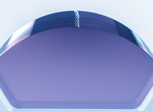
You might wonder how epitaxial wafers achieve their remarkable precision. The answer lies in advanced deposition techniques. These methods allow manufacturers to grow thin, uniform layers of crystalline material on a substrate. Chemical Vapor Deposition (CVD) is one of the most widely used techniques. It involves introducing reactive gases into a chamber, where they form a solid layer on the wafer’s surface. This process ensures high purity and excellent control over thickness.
Molecular Beam Epitaxy (MBE) is another cutting-edge method. It uses beams of atoms or molecules in a vacuum to deposit layers with atomic-level precision. This technique is ideal for creating complex structures, such as those needed in quantum computing or high-frequency devices. By refining these deposition methods, you can expect epitaxial wafers to meet even stricter performance requirements in the future.
Tip: Deposition techniques are the foundation of epitaxial wafer manufacturing. Understanding them helps you appreciate the technology behind modern electronics.
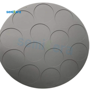
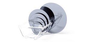
Larger Wafer Sizes
The demand for larger wafer sizes has grown as industries push for higher efficiency and lower costs. Larger wafers allow manufacturers to produce more chips from a single substrate, reducing waste and improving scalability. Today, 200mm and 300mm wafers are standard in many applications. However, researchers are already exploring even larger sizes to meet future needs.
Scaling up wafer sizes presents challenges. Maintaining uniformity across a larger surface requires precise control during manufacturing. Despite these hurdles, advancements in equipment and processes have made it possible to produce larger epitaxial wafers with consistent quality. This progress benefits industries like consumer electronics and automotive manufacturing, where cost efficiency is critical.
Material Integration (SiC, GaN)
Material integration has revolutionized the capabilities of epitaxial wafers. Silicon Carbide (SiC) and Gallium Nitride (GaN) are two materials that have gained significant attention. SiC is known for its ability to handle high voltages and temperatures, making it ideal for power electronics and electric vehicles. GaN, on the other hand, excels in high-frequency applications, such as 5G networks and radar systems.
By integrating these materials into epitaxial wafers, you can achieve superior performance compared to traditional silicon-based wafers. For example, SiC-based wafers improve the efficiency of electric vehicle chargers, while GaN-based wafers enhance the speed and reliability of wireless communication. These innovations open new possibilities for industries that rely on high-performance semiconductors.
Note: The integration of materials like SiC and GaN highlights the versatility of epitaxial wafers. They are no longer limited to silicon but are evolving to meet diverse technological demands.
Industry Applications of Epitaxial Wafers

Epitaxial wafers have become essential in various industries, enabling advancements in technology that directly impact your daily life. From the devices you use to the vehicles you drive, these wafers are at the heart of innovation.
Consumer Electronics
You rely on consumer electronics for communication, entertainment, and productivity. Epitaxial wafers play a critical role in making these devices faster, smaller, and more efficient. Smartphones, for example, benefit from the precise material properties of these wafers. They enable the production of high-performance processors and memory chips, ensuring your phone runs smoothly and handles demanding tasks.
Televisions and gaming consoles also use epitaxial wafers to deliver stunning visuals and immersive experiences. The wafers support advanced display technologies like OLED and micro-LED, which provide vibrant colors and sharp images. By improving the performance of semiconductors, epitaxial wafers enhance the quality and functionality of the electronics you use every day.
Fun Fact: The epitaxial wafer technology behind your smartphone’s processor is also used in cutting-edge quantum computing research.
Automotive and EVs
The automotive industry has embraced epitaxial wafers to meet the growing demand for electric vehicles (EVs) and advanced driver-assistance systems (ADAS). These wafers enable the production of power electronics that manage energy efficiently, extending the range of EVs and reducing charging times. Silicon Carbide (SiC) epitaxial wafers, in particular, are ideal for handling the high voltages required in EVs.
ADAS, which includes features like lane-keeping assistance and adaptive cruise control, relies on sensors and processors built using epitaxial wafers. These components ensure accurate data processing and quick response times, enhancing safety on the road. As the automotive industry continues to innovate, you can expect epitaxial wafers to play an even bigger role in shaping the future of transportation.
Healthcare Devices
In healthcare, precision and reliability are crucial. Epitaxial wafers contribute to the development of medical devices that improve patient care and diagnostic accuracy. Imaging equipment like MRI and CT scanners use semiconductors made from these wafers to produce clear and detailed images. This helps doctors diagnose conditions more effectively.
Wearable health monitors, such as fitness trackers and smartwatches, also benefit from epitaxial wafer technology. These devices use sensors to track vital signs like heart rate and blood oxygen levels, providing you with valuable insights into your health. By enabling the miniaturization and efficiency of medical devices, epitaxial wafers are transforming the way healthcare is delivered.
Tip: The next time you use a fitness tracker, remember that epitaxial wafers are part of the technology that keeps you informed about your health.
Renewable Energy Systems
Renewable energy systems rely on advanced technologies to harness power from natural sources like the sun and wind. Epitaxial wafers play a crucial role in improving the efficiency and reliability of these systems. By enabling the production of high-performance semiconductors, they help you get the most out of renewable energy technologies.
One of the most significant applications of epitaxial wafers is in solar panels. Modern photovoltaic (PV) cells use these wafers to convert sunlight into electricity more efficiently. The precise material properties of epitaxial wafers allow manufacturers to create thinner, more efficient solar cells. This means you can generate more energy even in areas with limited sunlight.
Did you know? Solar panels made with epitaxial wafers can achieve higher energy conversion rates compared to traditional silicon-based panels.
Wind energy systems also benefit from epitaxial wafer technology. Wind turbines require advanced power electronics to convert and manage the electricity they generate. These electronics often use semiconductors made from materials like Silicon Carbide (SiC), which are integrated into epitaxial wafers. This integration ensures that wind turbines operate efficiently, even under harsh conditions.
In addition to solar and wind energy, epitaxial wafers contribute to energy storage systems. Batteries used in renewable energy setups depend on efficient power management. Epitaxial wafers enable the development of semiconductors that regulate energy flow, ensuring stable and reliable storage. This helps you store excess energy for use during periods of low generation, such as at night or on cloudy days.
Tip: When choosing renewable energy solutions, look for systems that incorporate advanced semiconductors. These often use epitaxial wafers to deliver better performance and durability.
The impact of epitaxial wafers on renewable energy systems extends beyond efficiency. They also support the development of smaller, more compact devices. This makes it easier to integrate renewable energy technologies into homes, businesses, and even portable applications. As a result, you can enjoy cleaner energy without compromising on convenience or space.
By driving innovation in renewable energy systems, epitaxial wafers are helping to create a more sustainable future. They enable technologies that reduce reliance on fossil fuels and lower carbon emissions. As these wafers continue to evolve, you can expect even greater advancements in renewable energy efficiency and accessibility.
Market Trends Driving Epitaxial Wafer Growth
5G and IoT Expansion
The rise of 5G networks and the Internet of Things (IoT) has created a demand for faster and more efficient semiconductors. You rely on these technologies for seamless connectivity in devices like smartphones, smart home systems, and industrial sensors. Epitaxial wafers play a key role in meeting these demands. They enable the production of high-frequency chips that support faster data transmission and lower latency.
IoT devices require compact and energy-efficient components. Epitaxial wafers allow manufacturers to create smaller chips with precise material properties. This ensures that your smart devices consume less power while maintaining high performance. As 5G and IoT continue to expand, epitaxial wafers will remain essential for supporting these technologies.
Tip: When exploring IoT solutions, look for devices powered by advanced semiconductors. These often use epitaxial wafers for better efficiency.
EV and Power Electronics Demand
Electric vehicles (EVs) and power electronics are transforming transportation and energy systems. You see this in the growing popularity of EVs and renewable energy setups. Epitaxial wafers contribute to this transformation by enabling the production of power semiconductors that handle high voltages and temperatures.
In EVs, these wafers improve the efficiency of inverters and chargers, helping you drive farther on a single charge. Power electronics in renewable energy systems also benefit from epitaxial wafer technology. They ensure stable energy conversion and storage, making renewable energy more reliable.
Did you know? Silicon Carbide (SiC) epitaxial wafers are widely used in EVs for their ability to handle extreme conditions.
High-Performance Semiconductor Needs
Modern industries demand semiconductors that deliver exceptional speed and reliability. You see this need in applications like artificial intelligence, quantum computing, and advanced imaging systems. Epitaxial wafers meet these requirements by providing precise control over material properties.
These wafers enable the production of processors and sensors that operate at high frequencies. This improves the performance of devices ranging from supercomputers to medical imaging equipment. As industries push for higher performance, epitaxial wafers will continue to drive innovation.
Note: High-performance semiconductors made with epitaxial wafers are shaping the future of technology across multiple sectors.
Challenges and Future of Epitaxial Wafers
Cost and Scalability
Epitaxial wafers offer advanced capabilities, but their production costs remain high. You might wonder why this is the case. The answer lies in the precision required during manufacturing. Techniques like Chemical Vapor Deposition (CVD) and Molecular Beam Epitaxy (MBE) demand specialized equipment and skilled operators. These factors increase expenses, making it challenging for manufacturers to scale production.
Scalability also presents hurdles. As industries demand larger wafer sizes, maintaining uniformity across the surface becomes more difficult. This requires constant innovation in equipment and processes. Despite these challenges, researchers are exploring ways to reduce costs and improve scalability. For example, automation and AI-driven quality control systems are helping manufacturers streamline production.
Tip: Advances in automation could make epitaxial wafers more affordable and accessible in the future.
Sustainability Concerns
The environmental impact of epitaxial wafer production is another challenge. Manufacturing processes consume significant energy and generate waste materials. You might not realize it, but the chemicals used in deposition techniques can harm the environment if not managed properly.
To address these concerns, companies are adopting greener practices. Recycling materials and using renewable energy sources in production are becoming more common. Some manufacturers are even exploring eco-friendly alternatives to traditional chemicals. These efforts aim to reduce the carbon footprint of epitaxial wafer production.
Did you know? Sustainable manufacturing practices can make epitaxial wafers a key component in building a greener future.
Emerging Technologies
Emerging technologies are shaping the future of epitaxial wafers. Quantum computing, artificial intelligence, and advanced imaging systems require semiconductors with exceptional precision. You’ll see epitaxial wafers playing a critical role in these fields.
For example, quantum computers need wafers with atomic-level accuracy to function effectively. AI systems rely on high-performance processors, which epitaxial wafers enable. In imaging, these wafers support sensors that capture detailed visuals for medical and industrial applications.
Note: As new technologies emerge, epitaxial wafers will continue to evolve, driving innovation across industries.
Epitaxial wafer technology continues to redefine modern industries. Innovations like advanced deposition techniques, larger wafer sizes, and material integration have unlocked new possibilities. These advancements enable you to experience faster devices, safer vehicles, and cleaner energy systems.
Key Takeaway: Epitaxial wafers are not just components; they are the backbone of technological progress.
As industries evolve, these wafers will drive breakthroughs in quantum computing, AI, and renewable energy. By embracing this technology, you contribute to a future powered by efficiency, sustainability, and innovation.
FAQ
What are epitaxial wafers used for?
Epitaxial wafers are used in semiconductors for electronics, automotive systems, healthcare devices, and renewable energy. They improve performance, efficiency, and reliability in applications like processors, sensors, and power electronics.
Tip: Think of epitaxial wafers as the foundation for advanced technologies like 5G and electric vehicles.
How do epitaxial wafers differ from regular silicon wafers?
Epitaxial wafers have a thin, crystalline layer grown on their surface, offering precise control over material properties. Regular silicon wafers lack this layer, making epitaxial wafers better suited for high-performance applications like power electronics and quantum computing.
Why is Silicon Carbide (SiC) important in epitaxial wafers?
SiC handles high voltages and temperatures, making it ideal for electric vehicles and renewable energy systems. It boosts efficiency and durability in power electronics, enabling faster charging and better energy conversion.
Did you know? SiC epitaxial wafers are key to extending EV range and reducing energy waste.
Are epitaxial wafers environmentally friendly?
Manufacturing epitaxial wafers consumes energy and produces waste. However, companies are adopting greener practices like recycling materials and using renewable energy. These efforts aim to reduce the environmental impact of production.
What industries benefit most from epitaxial wafers?
Industries like consumer electronics, automotive, healthcare, and renewable energy benefit the most. Epitaxial wafers enable faster devices, safer vehicles, precise medical imaging, and efficient solar panels.
Fun Fact: Your smartphone, EV, and solar panel likely use epitaxial wafer technology!
| Contact Us To Get Better Information |
| By:semicera |
| Address : No. 1958 Jiangnan Road, Ningbo High tech Zone, Zhejiang Province, 315201, China |
| E-mail : sales01@semi-cera.com |
| E-mail : sales05@semi-cera.com |
| Tel : 86-0574-8650 3783 |
| Phone : 86-13373889683 |
| Skype : xianeryeah@outlook.com |
| Whatsapp : 86-13373889683 |
| Xing:https://www.xing.com/discover/your-posts |
| Pinterest:https://www.pinterest.com/Semicera/ |
| Facebook:https://www.facebook.com/profile.php?id=61575124466678 |
| Youtube:https://www.youtube.com/@Semicera |