Epitaxy, a crucial process in semiconductor technology, involves growing a crystalline layer on a substrate, where the new layer replicates the structure of the underlying material. To fully grasp epitaxy meaning, it’s essential to understand the epitaxy definition: a method that ensures precise control over material properties, enabling the production of high-quality layers for advanced electronic devices. Understanding what is epitaxy highlights its role in enhancing device performance, such as creating faster processors and brighter LEDs. Mastering Epitaxy in Semiconductor is fundamental to driving innovation in modern technology.
Key Takeaways
- Epitaxy is a way to grow a thin crystal layer on a base. This helps make better materials for electronics.
- There are two types of epitaxy. Homoepitaxy uses the same material for the layer and base. Heteroepitaxy uses different materials.
- Epitaxy improves devices by making smooth layers without defects. This helps create faster chips and brighter lights.
- Methods like vapor-phase epitaxy (VPE) and molecular beam epitaxy (MBE) control layer thickness and material mix.
- Epitaxy is important for modern tech. It powers tools in telecom, green energy, and medicine.
Understanding Epitaxy in Semiconductor
Definition and significance of epitaxy
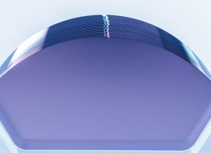
Epitaxy refers to the process of growing a thin crystalline layer on a substrate, where the new layer mimics the crystal structure of the base material. This technique plays a vital role in semiconductor manufacturing. It allows you to create high-quality materials with precise control over their properties. By using epitaxy, manufacturers can produce layers that are free from defects, ensuring better performance in electronic devices.
The significance of epitaxy lies in its ability to enhance the functionality of semiconductors. For example, it helps improve the efficiency of microchips, making them faster and more reliable. It also enables the creation of advanced devices like LEDs and lasers. Without epitaxy, many modern technologies would not function as efficiently as they do today.
Homoepitaxy vs. heteroepitaxy
Epitaxy can be classified into two main types: homoepitaxy and heteroepitaxy. In homoepitaxy, the crystalline layer and the substrate are made of the same material. For instance, growing a silicon layer on a silicon substrate is an example of homoepitaxy. This method is often used when you need to improve the quality of the existing material or add specific properties to it.
Heteroepitaxy, on the other hand, involves growing a crystalline layer on a substrate made of a different material. For example, depositing gallium arsenide on a silicon substrate falls under heteroepitaxy. This approach is useful when you want to combine the unique properties of two different materials. It is commonly used in applications like optoelectronics, where materials with different characteristics are needed to achieve specific results.
| Type of Epitaxy | Material Relationship | Example |
|---|---|---|
| Homoepitaxy | Same material | Silicon on silicon |
| Heteroepitaxy | Different materials | Gallium arsenide on silicon |
Key characteristics of epitaxial growth
Epitaxial growth has several key characteristics that make it essential for semiconductor manufacturing. First, it ensures that the new layer has a uniform and defect-free structure. This uniformity is crucial for creating reliable and efficient electronic components. Second, epitaxy allows you to control the thickness and composition of the layer with high precision. This level of control is necessary for designing advanced devices with specific functionalities.
Another important characteristic is the ability to grow layers at the atomic level. Techniques like molecular beam epitaxy (MBE) enable you to deposit materials one atom at a time, ensuring unmatched precision. Additionally, epitaxial growth supports the integration of different materials, which is essential for developing complex devices like transistors and sensors.
Tip: Understanding the characteristics of epitaxial growth can help you appreciate its role in creating the high-performance devices you use every day.
Types of Epitaxy in Semiconductor
Vapor-phase epitaxy (VPE)
Vapor-phase epitaxy (VPE) uses gases to deposit a crystalline layer on a substrate. You start by introducing a mixture of chemical vapors into a reaction chamber. These vapors react and form a thin layer on the substrate. This method works well for creating high-quality layers with precise control over thickness and composition.
VPE is popular because it operates at relatively low temperatures. This reduces the risk of damaging the substrate. It also allows you to grow layers with fewer defects, which is essential for reliable electronic devices. Manufacturers often use VPE for applications like transistors and diodes, where material quality directly impacts performance.
Note: VPE is ideal for large-scale production due to its efficiency and ability to handle multiple substrates simultaneously.
Molecular beam epitaxy (MBE)
Molecular beam epitaxy (MBE) offers unmatched precision for growing crystalline layers. In this technique, you use beams of atoms or molecules to deposit material onto a substrate. The process takes place in a vacuum chamber, ensuring a clean environment for crystal growth.
MBE allows you to control the growth at the atomic level. This makes it perfect for creating advanced devices like lasers and high-speed transistors. Although MBE is slower than other methods, its precision makes it invaluable for research and specialized applications.
Tip: If you need ultra-thin layers with exact compositions, MBE is the go-to method.
Liquid-phase epitaxy (LPE)
Liquid-phase epitaxy (LPE) involves using a liquid solution to grow a crystalline layer. You immerse the substrate in the solution, where the material gradually deposits onto its surface. This method is simple and cost-effective, making it suitable for certain applications.
LPE works best for growing thick layers or materials that are difficult to deposit using other techniques. You’ll often find it used in optoelectronic devices like LEDs and photodetectors. While it lacks the precision of MBE, LPE remains a practical choice for specific needs.
Alert: LPE is less common today but still plays a role in niche applications requiring thick or specialized layers.
Metal-organic chemical vapor deposition (MOCVD)
Metal-organic chemical vapor deposition (MOCVD) is a widely used technique for growing high-quality crystalline layers. In this method, you introduce metal-organic compounds and other gases into a reaction chamber. These compounds decompose on the heated substrate, forming a thin, uniform layer of material. The process takes place under controlled conditions, ensuring precise growth.
MOCVD stands out for its ability to produce layers with excellent uniformity and purity. You can grow complex structures, such as multi-layered materials, with ease. This makes it ideal for creating advanced semiconductor devices. The technique also allows you to control the composition and thickness of the layers, which is essential for designing custom materials.
One of the key advantages of MOCVD is its scalability. You can use it for both research and large-scale production. It is commonly employed in the manufacturing of LEDs, lasers, and high-performance transistors. The method’s versatility also makes it suitable for producing materials used in optoelectronics and power electronics.
Tip: MOCVD is a go-to choice when you need high-quality layers for demanding applications. Its precision and scalability make it a cornerstone of epitaxy in semiconductor manufacturing.
By mastering MOCVD, you can unlock new possibilities in device performance and innovation. This technique plays a crucial role in advancing modern technology.
The Epitaxy Process

Overview of epitaxial growth
Epitaxial growth is the process of depositing a crystalline layer on a substrate while maintaining the same crystal structure. This technique ensures that the new layer aligns perfectly with the substrate, creating a seamless and defect-free material. You can think of it as building a second floor on a house where every brick matches the foundation below.
This process happens under controlled conditions to achieve high precision. By carefully managing factors like temperature and material composition, you can grow layers with specific properties. These layers are essential for creating advanced semiconductor devices, such as microchips and LEDs. Epitaxial growth allows you to design materials that meet the exact needs of modern technology.
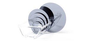
Role of substrates in epitaxy
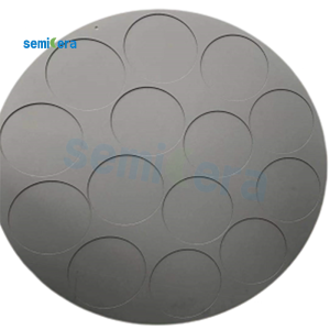
The substrate plays a critical role in epitaxy. It serves as the foundation for the crystalline layer, guiding its growth and structure. The quality of the substrate directly impacts the quality of the epitaxial layer. A smooth and defect-free substrate ensures better alignment and fewer imperfections in the final material.
You must also consider the compatibility between the substrate and the material being deposited. For example, in homoepitaxy, the substrate and the layer are made of the same material, ensuring perfect alignment. In heteroepitaxy, the materials differ, so you need to carefully match their properties to avoid issues like strain or defects. Choosing the right substrate is key to achieving successful epitaxial growth.
Techniques for controlling crystal growth
Controlling crystal growth is essential for producing high-quality epitaxial layers. You can use several techniques to manage this process. One common method is adjusting the temperature in the reaction chamber. Higher temperatures can speed up growth, while lower temperatures allow for more precise control.
Another technique involves regulating the flow of gases or materials during deposition. For example, in molecular beam epitaxy, you can control the rate at which atoms or molecules are deposited, ensuring atomic-level precision. Monitoring the environment, such as maintaining a vacuum or controlling pressure, also helps achieve consistent results.
By mastering these techniques, you can create materials with the exact properties needed for advanced applications. This level of control is what makes epitaxy in semiconductor manufacturing so valuable.
Benefits of Epitaxy in Semiconductor Manufacturing
Enhanced material purity and quality
Epitaxy allows you to create materials with exceptional purity and structural quality. By carefully controlling the growth process, you can eliminate defects and impurities that often occur in traditional manufacturing methods. This precision ensures that the crystalline layers you produce are uniform and free from inconsistencies.
High material purity is essential for advanced semiconductor devices. Impurities can disrupt the flow of electrons, reducing the efficiency of components like transistors and diodes. With epitaxy, you can achieve the level of purity needed for high-performance electronics.
Tip: If you aim to manufacture reliable and efficient devices, focusing on material quality through epitaxy is a must.
Improved device performance
Epitaxy in semiconductor manufacturing directly impacts the performance of electronic devices. By growing defect-free layers, you can enhance the electrical and optical properties of materials. This improvement translates to faster microprocessors, brighter LEDs, and more efficient power devices.
For example, epitaxial layers in microchips reduce resistance, allowing signals to travel faster. In optoelectronics, epitaxy ensures that light-emitting devices like lasers and LEDs operate with greater brightness and efficiency. The ability to fine-tune material properties gives you a competitive edge in creating cutting-edge technology.
Note: Devices built with epitaxial layers often last longer and perform better under demanding conditions.
Customization for advanced applications
One of the most significant advantages of epitaxy is its ability to customize materials for specific applications. You can control the thickness, composition, and structure of the layers to meet the unique requirements of your project. This flexibility is invaluable for developing specialized devices like high-frequency transistors or quantum computing components.
Epitaxy also enables you to combine different materials in a single device. For instance, heteroepitaxy allows you to integrate materials with distinct properties, such as silicon and gallium arsenide. This capability opens the door to innovations in fields like telecommunications, renewable energy, and medical technology.
Alert: Customization through epitaxy is key to staying ahead in industries that demand constant innovation.
Applications of Epitaxy in Semiconductor

Microprocessors and memory devices
Epitaxy plays a vital role in the production of microprocessors and memory devices. You rely on these components for everyday technologies like smartphones, computers, and gaming consoles. Epitaxial layers improve the performance of microchips by enhancing their electrical properties. This ensures faster data processing and efficient energy use.
In memory devices, epitaxy helps create high-density storage solutions. Manufacturers use it to grow defect-free layers that enable reliable data storage and retrieval. For example, dynamic random-access memory (DRAM) chips benefit from the precision of epitaxial growth. By using this technique, you can achieve higher speeds and greater storage capacities in modern devices.
Tip: The next time you use a fast-loading app or save a large file, remember that epitaxy might be behind its smooth performance.
Optoelectronic devices (e.g., LEDs, lasers)
Epitaxy is essential for optoelectronic devices like LEDs and lasers. These devices rely on materials with specific optical properties, which epitaxial growth can provide. For instance, you can use epitaxy to create layers of gallium arsenide or indium phosphide. These materials emit light efficiently, making them ideal for LEDs and laser diodes.
LEDs made with epitaxial layers shine brighter and last longer. Lasers, used in applications like fiber-optic communication and medical equipment, also benefit from the precision of epitaxy. By controlling the thickness and composition of the layers, you can produce devices with exceptional performance and reliability.
Note: Epitaxy in Semiconductor manufacturing has revolutionized the way optoelectronic devices are designed and produced.
Power electronics and RF devices
Power electronics and radio frequency (RF) devices also depend on epitaxy for their advanced capabilities. Power devices, such as those used in electric vehicles and renewable energy systems, require materials that can handle high voltages and currents. Epitaxial layers provide the necessary purity and structural integrity for these demanding applications.
In RF devices, like those found in smartphones and wireless communication systems, epitaxy ensures high-frequency performance. You can use heteroepitaxy to combine materials like silicon carbide and gallium nitride. This combination enhances efficiency and reduces energy loss, making RF devices more reliable and powerful.
Alert: Without epitaxy, many of the technologies you use daily, from 5G networks to electric cars, would not perform as efficiently.
Epitaxy stands as a cornerstone in semiconductor manufacturing. It lets you create materials with unmatched precision and quality, ensuring the reliability of modern electronic devices. By mastering epitaxy, you unlock the potential to design faster microprocessors, brighter LEDs, and more efficient power systems.
Note: Epitaxy doesn’t just improve today’s technology; it paves the way for future innovations like quantum computing and advanced telecommunications.
As industries demand smarter, faster, and more sustainable solutions, epitaxy will continue to shape the future of semiconductors. Its ability to customize materials for cutting-edge applications ensures that you stay ahead in a rapidly evolving technological landscape.
FAQ
What is the main purpose of epitaxy in semiconductor manufacturing?
Epitaxy helps you grow high-quality crystalline layers on substrates. This process ensures precise control over material properties, enabling the creation of advanced electronic devices like microchips, LEDs, and lasers. It improves performance, reliability, and efficiency in modern technology.
Tip: Think of epitaxy as the foundation for building better, faster, and smarter devices.
How does epitaxy differ from traditional material growth methods?
Epitaxy focuses on growing layers that mimic the substrate’s crystal structure. Traditional methods often lack this precision. With epitaxy, you achieve defect-free layers, better material purity, and tailored properties for specific applications, making it essential for high-performance electronics.
Why is substrate selection important in epitaxy?
The substrate acts as the foundation for crystal growth. Its quality and compatibility with the material being deposited directly affect the final layer’s performance. A smooth, defect-free substrate ensures better alignment and fewer imperfections in the epitaxial layer.
Note: Always match the substrate and material properties for optimal results.
Which industries benefit the most from epitaxy?
Epitaxy supports industries like consumer electronics, telecommunications, renewable energy, and healthcare. It powers devices such as microprocessors, LEDs, lasers, and power electronics. You’ll find epitaxy at the heart of innovations like 5G networks, electric vehicles, and medical imaging systems.
Can epitaxy enable future technologies like quantum computing?
Yes! Epitaxy allows you to create ultra-precise materials needed for quantum computing. By customizing layers at the atomic level, you can develop components like qubits, which are essential for quantum devices. This makes epitaxy a key player in shaping the future of technology.
Alert: Quantum computing relies on epitaxy for its groundbreaking advancements.
Contact Us To Get Better Information
By:semicera
Address : No. 1958 Jiangnan Road, Ningbo High tech Zone, Zhejiang Province, 315201, China
E-mail : sales01@semi-cera.com
E-mail : sales05@semi-cera.com
Tel : 86-0574-8650 3783
Phone : 86-13373889683
Skype : xianeryeah@outlook.com
Whatsapp : 86-13373889683
Xing:https://www.xing.com/discover/your-posts
Pinterest:https://www.pinterest.com/Semicera/
Facebook:https://www.facebook.com/profile.php?id=61575124466678
Youtube:https://www.youtube.com/@Semicera