Epitaxy has revolutionized the field of epitaxy semiconductor engineering, transforming how materials are crafted for advanced devices. But what is epitaxy? It’s a process where one material grows on another, replicating its atomic structure with remarkable precision. This epitaxy definition highlights its critical role in enabling semiconductors to operate faster and more efficiently. The epitaxy meaning Epitaxy extends beyond mere fabrication—it fuels innovation in areas like quantum computing and energy-efficient technologies. By understanding epitaxy definition, we unlock the potential to shape the future of semiconductor advancements.
Key Takeaways
- Epitaxy is an important method in making semiconductors. It helps grow materials carefully to improve how devices work and save energy.
- Gallium nitride (GaN) and silicon carbide (SiC) are special materials used in epitaxy. They help make powerful tools like electric cars and energy-saving gadgets.
- Selective area growth (SAG) lets scientists build tricky designs. It combines different materials on one chip for smarter devices.
- Epitaxy is key in quantum computing. It makes exact layers needed for qubits, helping this new technology grow.
- Using eco-friendly methods in epitaxy, like recycling and cooler processes, helps the planet and supports reusing resources.
The Foundations of Epitaxy
Defining Epitaxy
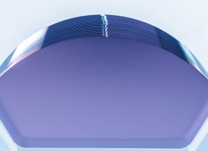
Epitaxy is a process where a thin layer of material grows on a substrate, mimicking its atomic structure. This technique allows you to create materials with precise properties, which are essential for advanced electronics. The term “epitaxy” comes from Greek, meaning “arranged upon.” It highlights how the new layer aligns perfectly with the underlying material. By controlling this growth, you can achieve the exact characteristics needed for specific applications, such as faster processors or energy-efficient devices.
Types of Epitaxy in Semiconductor Fabrication
In semiconductor fabrication, epitaxy comes in two main types: homoepitaxy and heteroepitaxy. Homoepitaxy involves growing a layer of material on a substrate of the same type. For example, silicon on silicon. This method ensures uniformity and is often used in high-performance devices. Heteroepitaxy, on the other hand, involves growing a layer on a different material. For instance, gallium nitride (GaN) on silicon. This approach enables you to combine the best properties of different materials, which is crucial for applications like LEDs and power electronics.
Importance of Epitaxy in Achieving Material Precision
Epitaxy plays a vital role in achieving the precision required in modern electronics. It allows you to control the thickness, composition, and crystal quality of the material layers. This precision is critical for creating devices that operate efficiently and reliably. For example, in epitaxy semiconductor processes, even a tiny defect can impact performance. By mastering epitaxy, you can ensure that devices meet the demanding standards of industries like telecommunications, automotive, and quantum computing.
Key Trends in Epitaxy Semiconductor Technology

Advancements in GaN and SiC Materials
Gallium nitride (GaN) and silicon carbide (SiC) have become game-changers in the epitaxy semiconductor industry. These materials offer unique properties that make them ideal for high-performance applications. GaN, for example, has a wide bandgap, which allows it to handle higher voltages and operate at faster speeds. This makes it perfect for devices like power amplifiers and LEDs. SiC, on the other hand, excels in high-temperature and high-power environments. It is widely used in electric vehicles and renewable energy systems.
You can see the impact of these materials in the growing demand for energy-efficient technologies. GaN and SiC-based devices reduce energy loss, which helps lower electricity consumption. This is especially important as industries aim to meet sustainability goals. The development of advanced epitaxy techniques has also improved the quality of GaN and SiC layers, reducing defects and enhancing performance. These advancements are paving the way for more reliable and efficient electronic devices.
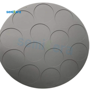
Selective Area Growth Techniques
Selective area growth (SAG) is another exciting trend in epitaxy semiconductor technology. This technique allows you to grow materials only in specific regions of a substrate. By using masks or templates, you can control where the material grows, creating intricate patterns and structures. This precision is essential for developing complex devices like photonic chips and microelectromechanical systems (MEMS).
One of the key benefits of SAG is its ability to integrate different materials on a single chip. For instance, you can combine silicon with GaN or other materials to create hybrid devices. This opens up new possibilities for miniaturization and multifunctionality. SAG also reduces material waste, making it a more sustainable option for semiconductor manufacturing. As you explore this technique, you’ll find it plays a crucial role in pushing the boundaries of modern electronics.
Tunnel Structures for Quantum Applications
Quantum computing is one of the most promising fields in technology today, and epitaxy semiconductor processes are at the heart of its development. Tunnel structures, which rely on quantum tunneling, are essential for creating qubits—the building blocks of quantum computers. These structures allow electrons to pass through barriers in ways that classical physics cannot explain. This phenomenon enables the creation of devices with unprecedented computational power.
Epitaxy is critical for fabricating these tunnel structures with the precision required for quantum applications. You can control the thickness and composition of the layers to ensure optimal performance. This level of control is vital for maintaining the delicate quantum states needed for computation. As quantum technology advances, the demand for high-quality epitaxial materials will continue to grow. By mastering these techniques, you can contribute to the next wave of innovation in computing.
Enhancing Power Electronics and Energy Efficiency
Power electronics play a crucial role in modern technology, from electric vehicles to renewable energy systems. Epitaxy has become a cornerstone in advancing these technologies by enabling the creation of high-performance materials. You can see its impact in devices designed to handle higher voltages, operate at faster speeds, and reduce energy loss.
One of the key benefits of epitaxy in power electronics is its ability to improve energy efficiency. Devices made with epitaxial layers, such as gallium nitride (GaN) and silicon carbide (SiC), experience less energy loss during operation. This means they generate less heat and require smaller cooling systems. For example, in electric vehicles, this translates to longer battery life and increased driving range.
Epitaxy also allows you to create thinner and more precise layers of material. This precision enhances the performance of power transistors and diodes, which are essential components in power conversion systems. By reducing defects in these layers, you can ensure that devices operate reliably under high-stress conditions.
Tip: When designing power electronics, consider using materials like GaN and SiC. These materials, enhanced through epitaxy, offer superior performance and energy savings.
Another advantage of epitaxy is its contribution to miniaturization. Smaller, more efficient devices are now possible because of advancements in epitaxy semiconductor processes. This is especially important in industries like telecommunications, where compact and energy-efficient components are in high demand.
The push for sustainability has also driven innovation in epitaxy. By improving material quality and reducing waste, epitaxy supports the development of greener technologies. You can expect to see more energy-efficient devices in the future, thanks to these advancements.
Challenges in Epitaxy Semiconductor Processes
Addressing Substrate Compatibility
Substrate compatibility remains one of the most significant challenges in epitaxy semiconductor processes. You need to ensure that the substrate material matches the properties of the epitaxial layer. When the lattice structures of the two materials differ, it creates strain, which can lead to defects. For example, growing gallium nitride (GaN) on silicon requires careful engineering to minimize mismatches.
To overcome this, you can use buffer layers or intermediate materials to bridge the gap between the substrate and the epitaxial layer. These layers help reduce strain and improve the overall quality of the material. Another approach involves selecting substrates with similar lattice structures to the epitaxial material. By addressing compatibility issues, you can achieve better performance and reliability in your devices.
Reducing Defect Density in Layers
Defects in epitaxial layers can significantly impact the performance of semiconductor devices. Even minor imperfections can disrupt the flow of electrons, reducing efficiency and reliability. You need to focus on minimizing defect density during the growth process.
One effective method involves optimizing growth conditions, such as temperature and pressure. These factors influence how atoms arrange themselves during epitaxy. Advanced techniques like molecular beam epitaxy (MBE) or metal-organic chemical vapor deposition (MOCVD) allow you to control these conditions with precision. Additionally, using high-quality substrates and buffer layers can further reduce defects. By prioritizing defect reduction, you can ensure your devices meet industry standards.
Managing Thermal Challenges in Devices
Thermal management is another critical aspect of epitaxy semiconductor processes. As devices become smaller and more powerful, heat generation increases. You need to address this issue to prevent overheating and ensure long-term reliability.
Materials like silicon carbide (SiC) and gallium nitride (GaN) excel in high-temperature environments. These materials, grown through epitaxy, offer better thermal conductivity and stability. You can also design thinner layers to improve heat dissipation. Incorporating advanced cooling systems into your devices can further enhance thermal management. By tackling these challenges, you can create devices that perform efficiently under demanding conditions.
Innovations in High-Purity Materials and Equipment
High-purity materials and advanced equipment have become essential for improving epitaxy processes. You need these innovations to achieve the precision required in modern semiconductor devices. Impurities in materials can lead to defects, which reduce the performance and reliability of your devices. By using high-purity materials, you can minimize these issues and create layers with exceptional quality.
One major advancement is the development of ultra-high-purity gases and chemicals. These materials ensure that the growth environment remains free from contaminants. For example, in processes like molecular beam epitaxy (MBE), the use of purified elements allows you to control the atomic structure of the layers with incredible accuracy. This level of control is critical for applications in quantum computing and high-frequency electronics.
Equipment innovations also play a key role. Modern epitaxy tools now feature advanced monitoring systems that let you track the growth process in real time. These systems use techniques like in-situ spectroscopy to detect even the smallest deviations. By identifying issues early, you can adjust parameters and maintain the quality of the layers.
Tip: When selecting equipment, look for systems with automated controls. These features can help you achieve consistent results and reduce production errors.
Another breakthrough is the use of specialized reactors designed for high-purity environments. These reactors prevent contamination and allow for uniform material deposition. You can use them to produce complex structures, such as multi-layered devices, with fewer defects. These advancements in materials and equipment are driving the epitaxy semiconductor industry forward, enabling the creation of next-generation technologies.
Applications of Epitaxy in Modern Electronics

Automotive Electronics and SmartSiC™
Epitaxy has transformed automotive electronics by enabling the development of advanced materials like silicon carbide (SiC). You can see its impact in electric vehicles (EVs), where SiC-based components improve energy efficiency and performance. SmartSiC™ technology, a breakthrough in this field, uses epitaxy to create high-quality SiC layers. These layers enhance the reliability of power modules, which are essential for EVs and hybrid vehicles.
SmartSiC™ technology allows you to achieve better thermal management in automotive electronics. SiC materials dissipate heat more effectively than traditional silicon, ensuring that devices operate reliably under high-stress conditions. This is especially important for EVs, where power modules handle high voltages and temperatures. By using epitaxy semiconductor processes, manufacturers can produce thinner and more precise SiC layers, reducing energy loss and extending battery life.
Another advantage of epitaxy in automotive electronics is its role in miniaturization. You can create smaller, more efficient components without compromising performance. This opens up new possibilities for integrating advanced features like autonomous driving systems and in-vehicle connectivity. As the automotive industry continues to innovate, epitaxy will remain a key driver of progress.
Telecommunications and 5G Advancements
Telecommunications rely heavily on epitaxy semiconductor technology to meet the demands of modern networks. You can see its influence in 5G advancements, where epitaxial materials enable faster data transmission and lower latency. Gallium nitride (GaN), a material grown through epitaxy, plays a crucial role in 5G infrastructure. It supports high-frequency signals, making it ideal for base stations and antennas.
Epitaxy allows you to create high-quality GaN layers with precise properties. These layers improve the efficiency of power amplifiers, which are essential for transmitting signals over long distances. By reducing energy loss, epitaxial GaN devices help lower operational costs and support sustainable practices in telecommunications.
Another benefit of epitaxy in 5G technology is its ability to integrate multiple functions on a single chip. You can combine different materials, such as GaN and silicon, to create hybrid devices that perform better and take up less space. This is critical for meeting the growing demand for compact and energy-efficient components in telecommunications.
Note: When designing 5G systems, consider using epitaxial materials like GaN. These materials offer superior performance and reliability, ensuring that your devices meet industry standards.
Micro-Displays and FD-SOI Technology
Micro-displays have become increasingly popular in applications like augmented reality (AR) and virtual reality (VR). Epitaxy plays a vital role in creating the high-resolution screens needed for these technologies. You can use epitaxy semiconductor processes to grow materials like indium gallium arsenide (InGaAs), which offer excellent optical properties. These materials enable brighter and more vibrant displays, enhancing the user experience.
Fully-depleted silicon-on-insulator (FD-SOI) technology is another area where epitaxy has made a significant impact. FD-SOI uses epitaxial layers to improve the performance of microprocessors and sensors. You can achieve better energy efficiency and faster processing speeds with this technology, making it ideal for portable devices like smartphones and wearables.
Epitaxy also supports the miniaturization of micro-displays and FD-SOI components. You can create thinner layers with fewer defects, ensuring that devices operate reliably even in demanding environments. This is particularly important for AR and VR applications, where compact and lightweight designs are essential.
As you explore the possibilities of epitaxy in micro-displays and FD-SOI technology, you’ll find that it opens up new opportunities for innovation. Whether you’re developing next-generation screens or advanced sensors, epitaxy provides the precision and reliability needed to succeed.
Quantum Computing and Emerging Devices
Quantum computing represents a leap forward in technology, offering computational power far beyond what classical computers can achieve. You can think of it as a new frontier where the rules of quantum mechanics enable breakthroughs in solving complex problems. Epitaxy semiconductor processes play a pivotal role in this field, especially in the creation of qubits—the fundamental units of quantum information.
How Epitaxy Enables Quantum Computing
Epitaxy allows you to fabricate ultra-thin layers of materials with precise atomic arrangements. These layers are essential for building quantum devices like tunnel junctions and quantum dots. For example, you can use epitaxy to grow materials such as indium arsenide (InAs) or gallium arsenide (GaAs), which exhibit the properties needed for quantum tunneling.
Note: Quantum tunneling is a phenomenon where particles pass through barriers that would be insurmountable in classical physics. This behavior is key to the operation of qubits.
Emerging Devices Powered by Epitaxy
Quantum computing isn’t the only area benefiting from epitaxy semiconductor advancements. You’ll find epitaxy at the heart of emerging devices like single-photon detectors and advanced sensors. These devices rely on epitaxial layers to achieve high sensitivity and precision.
Here’s a quick look at some applications:
- Single-Photon Detectors: Used in quantum communication and cryptography, these detectors require epitaxial materials to capture individual photons with minimal noise.
- Quantum Dots: These nanoscale structures, grown through epitaxy, are used in displays and biomedical imaging.
- Superconducting Qubits: Epitaxy enables the creation of superconducting materials that operate at extremely low temperatures, essential for quantum computing.
Challenges and Opportunities
Creating epitaxial layers for quantum devices isn’t without challenges. You need to address issues like defect density and material purity to ensure reliable performance. Innovations in epitaxy equipment and processes are helping overcome these hurdles. For instance, molecular beam epitaxy (MBE) offers unparalleled control over layer thickness and composition.
Tip: When working on quantum devices, prioritize high-purity materials and advanced epitaxy techniques. These factors are critical for achieving the precision required in quantum applications.
The Future of Quantum Devices
As quantum computing evolves, you’ll see epitaxy semiconductor processes driving the development of more advanced devices. Researchers are exploring new materials like topological insulators and 2D materials, which could revolutionize quantum technology. By mastering epitaxy, you can contribute to innovations that shape the future of computing and beyond.
The Future of Epitaxy Semiconductor Technology
Sustainable Manufacturing Practices
Sustainability has become a priority in the semiconductor industry. You can see this shift in the adoption of eco-friendly epitaxy processes. Manufacturers now focus on reducing energy consumption during material growth. For example, low-temperature epitaxy techniques help minimize the carbon footprint of production. These methods also lower operational costs, making them a win-win for both the environment and businesses.
Recycling plays a key role in sustainable practices. You can reuse substrates and other materials to reduce waste. Advanced cleaning technologies ensure that recycled components meet the same quality standards as new ones. This approach not only conserves resources but also supports a circular economy in the epitaxy semiconductor industry.
Innovations in Materials and Processes
New materials are reshaping the future of epitaxy. You can explore options like 2D materials, which offer unique electrical and optical properties. These materials, such as graphene and transition metal dichalcogenides, enable the creation of ultra-thin and flexible devices. They also open doors to applications in wearable electronics and advanced sensors.
Process innovations are equally transformative. Techniques like atomic layer epitaxy (ALE) allow you to grow materials one atomic layer at a time. This level of precision ensures defect-free layers, which are essential for high-performance devices. You can also benefit from real-time monitoring systems that provide instant feedback during material growth. These systems help maintain quality and reduce production errors.
Next-Generation Semiconductor Devices
Epitaxy is driving the development of next-generation devices. You can expect breakthroughs in areas like artificial intelligence (AI) and the Internet of Things (IoT). For instance, epitaxial layers improve the efficiency of AI processors, enabling faster data analysis. In IoT devices, these layers enhance connectivity and energy efficiency.
Miniaturization is another exciting trend. You can create smaller, more powerful chips using advanced epitaxy techniques. These chips are ideal for compact devices like smartphones and wearables. By mastering epitaxy semiconductor processes, you contribute to innovations that shape the future of technology.
Epitaxy has redefined how you approach semiconductor technology. It enables precise material engineering, which drives innovation across industries like automotive, telecommunications, and quantum computing. Its contributions to energy efficiency and miniaturization have transformed modern electronics. As you look ahead, epitaxy semiconductor advancements promise to unlock new possibilities in sustainable manufacturing and next-generation devices. By embracing these innovations, you can play a role in shaping the future of electronics and technology.
FAQ
What is epitaxy, and why is it important in semiconductors?
Epitaxy is the process of growing a material layer on a substrate with precise atomic alignment. It ensures high-quality layers for semiconductors, enabling faster devices, better energy efficiency, and advanced applications like quantum computing.
How does epitaxy improve energy efficiency in electronics?
Epitaxy creates defect-free layers of materials like GaN and SiC. These materials reduce energy loss during operation, leading to less heat generation and improved performance in devices like electric vehicles and power systems.
What are the main challenges in epitaxy processes?
You face challenges like substrate compatibility, defect density, and thermal management. Innovations in buffer layers, high-purity materials, and advanced equipment help overcome these issues and improve layer quality.
Can epitaxy be used in quantum computing?
Yes, epitaxy enables the creation of precise layers for quantum devices like qubits and tunnel junctions. These layers support quantum tunneling, which is essential for the operation of quantum computers.
What materials are commonly used in epitaxy?
Materials like silicon, gallium nitride (GaN), silicon carbide (SiC), and indium gallium arsenide (InGaAs) are widely used. Each material offers unique properties suited for applications like power electronics, telecommunications, and quantum devices.
Contact Us To Get Better Information |
| By:semicera |
| Address : No. 1958 Jiangnan Road, Ningbo High tech Zone, Zhejiang Province, 315201, China |
| E-mail : sales01@semi-cera.com |
| E-mail : sales05@semi-cera.com |
| Tel : 86-0574-8650 3783 |
| Phone : 86-13373889683 |
| Skype : xianeryeah@outlook.com |
| Whatsapp : 86-13373889683 |
| Xing:semicera |
| Pinterest:semicera |
| Facebook:semicera |
| Youtube:semicera |