Silicon carbide (SiC) single crystal material has a large band gap width (~Si 3 times), high thermal conductivity (~Si 3.3 times or GaAs 10 times), high electron saturation migration rate (~Si 2.5 times), high breakdown electric field (~Si 10 times or GaAs 5 times) and other outstanding characteristics.
De halfgeleider -materialen van de derde generatie omvatten voornamelijk SIC, GAN, Diamond, enz., Omdat de bandafstandbreedte (bijv.) Groter is dan of gelijk is aan 2,3 elektronenvolt (EV), ook bekend als brede band gap semiconductor -materialen. Vergeleken met de eerste en tweede generatie halfgeleidermaterialen, hebben de halfgeleidermaterialen van de derde generatie de voordelen van een hoge thermische geleidbaarheid, elektrisch veld met hoge afbraak, hoge verzadigde elektronenmigratiesnelheid en hoge bindingsergie, die kunnen voldoen aan de nieuwe vereisten van moderne elektronische technologie voor hoge temperatuur, hoog vermogen, hoge druk, hoge frequentie en bestraling resistentie en andere HARSH -omstandigheden. Het heeft belangrijke toepassingsperspectieven op het gebied van nationale verdediging, luchtvaart, ruimtevaart, olie -exploratie, optische opslag, enz., En kan energieverlies verminderen met meer dan 50% in veel strategische industrieën zoals breedbandcommunicatie, zonne -energie, automobielproductie, halfgeleiderverlichting en smart grid en smart grid en smart grid en smart grid.
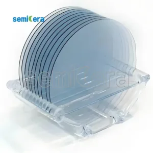
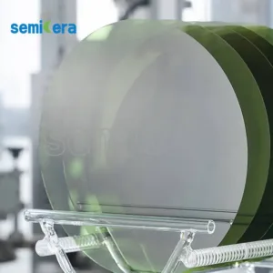
Semicera energy can provide customers with high-quality Conductive (Conductive), Semi-insulating (Semi-insulating), HPSI (High Purity semi-insulating) silicon carbide substrate; In addition, we can provide customers with homogeneous and heterogeneous silicon carbide epitaxial sheets; We can also customize the epitaxial sheet according to the specific needs of customers, and there is no minimum order quantity.
|
Maat |
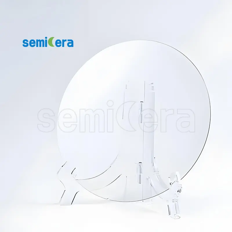
6-inch |
| Diameter | 150.0mm+0mm/-0.2mm |
| Oppervlakte -oriëntatie | off-axis:4°toward<1120>±0.5° |
| Primary Flat Length | 47.5mm1.5 mm |
| Primary Flat Orientation | <1120>±1.0° |
| Secundaire flat | Geen |
| Dikte | 350.0um±25.0um |
| Polytype | 4H |
| Geleidend type | n-type |
| 6-inch | ||
| Item | P-MOS Grade | P-SBD Grade |
| Weerstand | 0.015Ω·cm-0.025Ω·cm | |
| Polytype | None permitted | |
| Micropipe Density | ≤0.2/cm2 | ≤0.5/cm2 |
| EPD | ≤4000/cm2 | ≤8000/cm2 |
| TED | ≤3000/cm2 | ≤6000/cm2 |
| BPD | ≤1000/cm2 | ≤2000/cm2 |
| TSD | ≤300/cm2 | ≤1000/cm2 |
| SF(Measured byUV-PL-355nm) | ≤0.5% area | ≤1% area |
| Hex plates by high intensity light | None permitted | |
| Visual CarbonInclusions by high intensity light | Cumulativearea≤0.05% | |