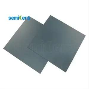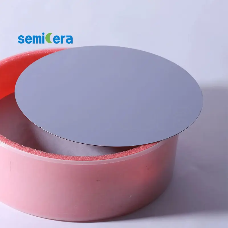
Semicera introduces the 850V High Power Gan-on-Si Epi Wafer, a breakthrough in semiconductor innovation. This advanced epi wafer combines the high efficiency of Gallium Nitride (GaN) with the cost-effectiveness of Silicon (Si), creating a powerful solution for high-voltage applications.
Belangrijke functies:
• High Voltage Handling: Engineered to support up to 850V, this GaN-on-Si Epi Wafer is ideal for demanding power electronics, enabling higher efficiency and performance.
• Enhanced Power Density: With superior electron mobility and thermal conductivity, GaN technology allows for compact designs and increased power density.
• Cost-Effective Solution: By leveraging silicon as the substrate, this epi wafer offers a cost-effective alternative to traditional GaN wafers, without compromising on quality or performance.
• Wide Application Range: Perfect for use in power converters, RF amplifiers, and other high-power electronic devices, ensuring reliability and durability.
Explore the future of high-voltage technology with Semicera’s 850V High Power Gan-on-Si Epi Wafer. Designed for cutting-edge applications, this product ensures your electronic devices operate with maximum efficiency and reliability. Choose Semicera for your next-generation semiconductor needs.
|
Items |
Productie |
Onderzoek |
Stom |
|
Kristalparameters |
|||
|
Polytype |
4H |
||
|
Oppervlakte -oriëntatiefout |
4±0.15° |
||
|
Elektrische parameters |
|||
|
Dopant |
n-type stikstof |
||
|
Weerstand |
0.015-0.025OHM · cm |
||
|
Mechanische parameters |
|||
|
Diameter |
150,0 ± 0,2 mm |
||
|
Dikte |
350 ± 25 µm |
||
|
Primaire platte oriëntatie |
[1-100]±5° |
||
|
Primaire platte lengte |
47,5 ± 1,5 mm |
||
|
Secundaire flat |
Geen |
||
|
TTV |
≤5 µm |
≤10 µm |
≤15 µm |
|
LTV |
≤3 μm (5 mm*5 mm) |
≤5 μm (5 mm*5 mm) |
≤10 μm (5 mm*5 mm) |
|
Boog |
-15 μm ~ 15 μm |
-35 μm ~ 35 μm |
-45μm ~ 45 urm |
|
Kronkelen |
≤35 µm |
≤45 µm |
≤55 µm |
|
Voorste (si-face) ruwheid (AFM) |
Ra≤0,2 nm (5μm*5μm) |
||
|
Structuur |
|||
|
Micropipe dichtheid |
<1 EA/CM2 |
<10 EA/CM2 |
<15 EA/CM2 |
|
Metaalonzuiverheden |
≤5E10atoms/cm2 |
NA |
|
|
BPD |
≤1500 EA/CM2 |
≤3000 EA/CM2 |
NA |
|
TSD |
≤500 EA/CM2 |
≤1000 EA/CM2 |
NA |
|
Voorste kwaliteit |
|||
|
Voorkant |
Si |
||
|
Oppervlakte -afwerking |
Si-face CMP |
||
|
Deeltjes |
≤60EA/wafer (grootte ≥ 0,3 μm) |
NA |
|
|
Krassen |
≤5EA/mm. Cumulatieve lengte ≤diameter |
Cumulatieve lengte ≤2*diameter |
NA |
|
Sinaasappelschil/putten/vlekken/strepen/scheuren/besmetting |
Geen |
NA |
|
|
Edge -chips/inspringen/breuk/hexplaten |
Geen |
||
|
Polytype -gebieden |
Geen |
Cumulatief gebied ≤20% |
Cumulatief gebied ≤30% |
|
Laser markering vooraan |
Geen |
||
|
Rugkwaliteit |
|||
|
Back Finish |
C-gezicht CMP |
||
|
Krassen |
≤5ea/mm, cumulatieve lengte ≤2*diameter |
NA |
|
|
Achterafwijkingen (randchips/inspringen) |
Geen |
||
|
Terug ruwheid |
Ra≤0,2 nm (5μm*5μm) |
||
|
Lasergrondbekleding |
1 mm (van bovenrand) |
||
|
Rand |
|||
|
Rand |
Schuif |
||
|
Verpakking |
|||
|
Verpakking |
Epi-ready met vacuümverpakkingen Multi-wafer cassette verpakking |
||
|
*OPMERKINGEN: "NA" betekent dat er geen aanvraagitems die niet worden genoemd, verwijzen naar semi-STD. |
|||