Semicera proudly offers GA2O3 Epitaxy, a state-of-the-art solution designed to push the boundaries of power electronics and optoelectronics. This advanced epitaxial technology leverages the unique properties of Gallium Oxide (Ga2O3) to deliver superior performance in demanding applications.
Belangrijke functies:
• Exceptional Wide Bandgap: GA2O3 Epitaxy features an ultra-wide bandgap, allowing for higher breakdown voltages and efficient operation in high-power environments.
• High Thermal Conductivity: The epitaxial layer provides excellent thermal conductivity, ensuring stable operation even under high-temperature conditions, making it ideal for high-frequency devices.
• Superieure materiaalkwaliteit: Achieve high crystal quality with minimal defects, ensuring optimal device performance and longevity, especially in critical applications such as power transistors and UV detectors.
• Veelzijdigheid in toepassingen: Perfectly suited for power electronics, RF applications, and optoelectronics, providing a reliable foundation for next-generation semiconductor devices.
Discover the potential of GA2O3 Epitaxy with Semicera’s innovative solutions. Our epitaxial products are designed to meet the highest standards of quality and performance, enabling your devices to operate with maximum efficiency and reliability. Choose Semicera for cutting-edge semiconductor technology.
|
Items |
Productie |
Onderzoek |
Stom |
|
Kristalparameters |
|||
|
Polytype |
4H |
||
|
Oppervlakte -oriëntatiefout |
4±0.15° |
||
|
Elektrische parameters |
|||
|
Dopant |
n-type stikstof |
||
|
Weerstand |
0.015-0.025OHM · cm |
||
|
Mechanische parameters |
|||
|
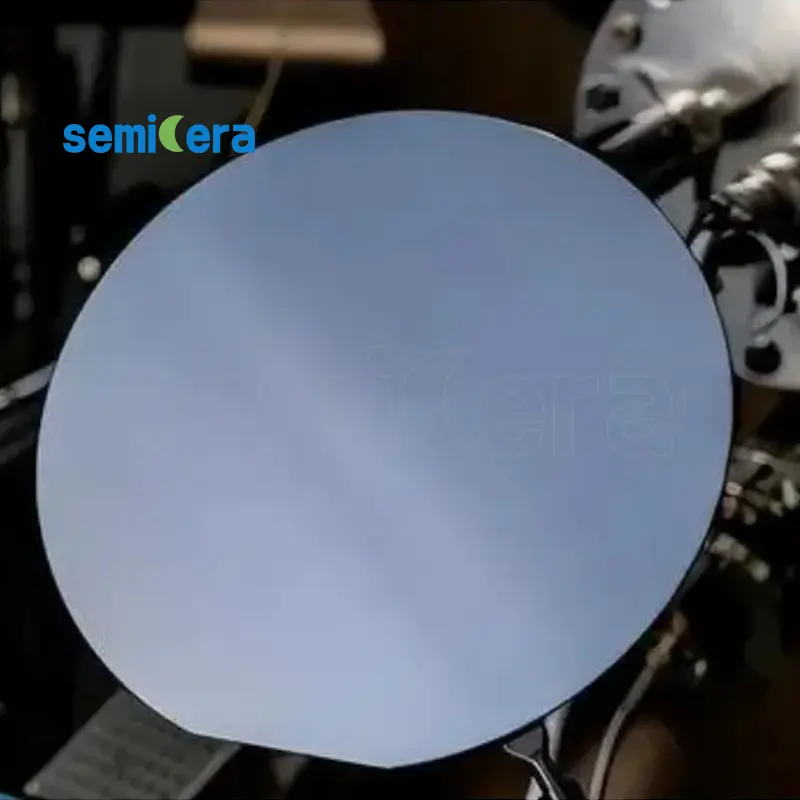
Diameter |
150,0 ± 0,2 mm |
||
|
Dikte |
350 ± 25 µm |
||
|
Primaire platte oriëntatie |
[1-100]±5° |
||
|
Primaire platte lengte |
47,5 ± 1,5 mm |
||
|
Secundaire flat |
Geen |
||
|
TTV |
≤5 µm |
≤10 µm |
≤15 µm |
|
LTV |
≤3 μm (5 mm*5 mm) |
≤5 μm (5 mm*5 mm) |
≤10 μm (5 mm*5 mm) |
|
Boog |
-15 μm ~ 15 μm |
-35 μm ~ 35 μm |
-45μm ~ 45 urm |
|
Kronkelen |
≤35 µm |
≤45 µm |
≤55 µm |
|
Voorste (si-face) ruwheid (AFM) |
Ra≤0,2 nm (5μm*5μm) |
||
|
Structuur |
|||
|
Micropipe dichtheid |
<1 EA/CM2 |
<10 EA/CM2 |
<15 EA/CM2 |
|
Metaalonzuiverheden |
≤5E10atoms/cm2 |
NA |
|
|
BPD |
≤1500 EA/CM2 |
≤3000 EA/CM2 |
NA |
|
TSD |
≤500 EA/CM2 |
≤1000 EA/CM2 |
NA |
|
Voorste kwaliteit |
|||
|
Voorkant |
Si |
||
|
Oppervlakte -afwerking |
Si-face CMP |
||
|
Deeltjes |
≤60EA/wafer (grootte ≥ 0,3 μm) |
NA |
|
|
Krassen |
≤5EA/mm. Cumulatieve lengte ≤diameter |
Cumulatieve lengte ≤2*diameter |
NA |
|
Sinaasappelschil/putten/vlekken/strepen/scheuren/besmetting |
Geen |
NA |
|
|
Edge -chips/inspringen/breuk/hexplaten |
Geen |
||
|
Polytype -gebieden |
Geen |
Cumulatief gebied ≤20% |
Cumulatief gebied ≤30% |
|
Laser markering vooraan |
Geen |
||
|
Rugkwaliteit |
|||
|
Back Finish |
C-gezicht CMP |
||
|
Krassen |
≤5ea/mm, cumulatieve lengte ≤2*diameter |
NA |
|
|
Achterafwijkingen (randchips/inspringen) |
Geen |
||
|
Terug ruwheid |
Ra≤0,2 nm (5μm*5μm) |
||
|
Lasergrondbekleding |
1 mm (van bovenrand) |
||
|
Rand |
|||
|
Rand |
Schuif |
||
|
Verpakking |
|||
|
Verpakking |
Epi-ready met vacuümverpakkingen Multi-wafer cassette verpakking |
||
|
*OPMERKINGEN: "NA" betekent dat er geen aanvraagitems die niet worden genoemd, verwijzen naar semi-STD. |
|||


