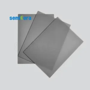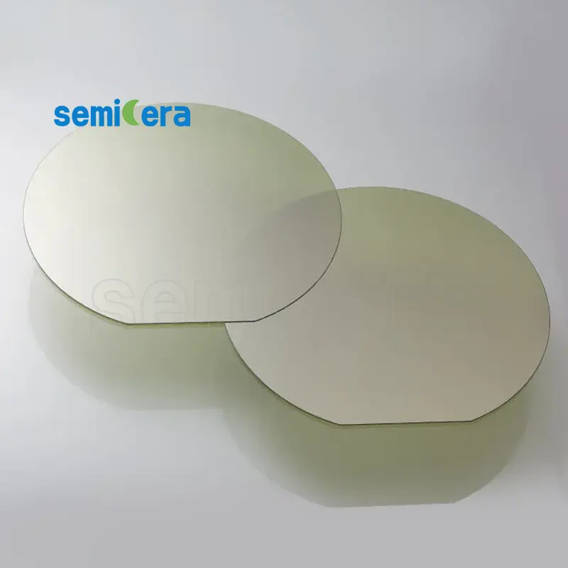
Semicera’s P-type SiC Substrate Wafer is a key component for developing advanced electronic and optoelectronic devices. These wafers are specifically designed to provide enhanced performance in high-power and high-temperature environments, supporting the growing demand for efficient and durable components.
The P-type doping in our SiC wafers ensures improved electrical conductivity and charge carrier mobility. This makes them particularly suitable for applications in power electronics, LEDs, and photovoltaic cells, where low power loss and high efficiency are critical.
Manufactured with the highest standards of precision and quality, Semicera’s P-type SiC wafers offer excellent surface uniformity and minimal defect rates. These characteristics are vital for industries where consistency and reliability are essential, such as aerospace, automotive, and renewable energy sectors.
Semicera’s commitment to innovation and excellence is evident in our P-type SiC Substrate Wafer. By integrating these wafers into your production process, you ensure that your devices benefit from the exceptional thermal and electrical properties of SiC, enabling them to operate effectively under challenging conditions.
Investing in Semicera’s P-type SiC Substrate Wafer means choosing a product that combines cutting-edge material science with meticulous engineering. Semicera is dedicated to supporting the next generation of electronic and optoelectronic technologies, providing the essential components needed for your success in the semiconductor industry.
|
Items |
Productie |
Onderzoek |
Stom |
|
Kristalparameters |
|||
|
Polytype |
4H |
||
|
Oppervlakte -oriëntatiefout |
4±0.15° |
||
|
Elektrische parameters |
|||
|
Dopant |
n-type stikstof |
||
|
Weerstand |
0.015-0.025OHM · cm |
||
|
Mechanische parameters |
|||
|
Diameter |
150,0 ± 0,2 mm |
||
|
Dikte |
350 ± 25 µm |
||
|
Primaire platte oriëntatie |
[1-100]±5° |
||
|
Primaire platte lengte |
47,5 ± 1,5 mm |
||
|
Secundaire flat |
Geen |
||
|
TTV |
≤5 µm |
≤10 µm |
≤15 µm |
|
LTV |
≤3 μm (5 mm*5 mm) |
≤5 μm (5 mm*5 mm) |
≤10 μm (5 mm*5 mm) |
|
Boog |
-15 μm ~ 15 μm |
-35 μm ~ 35 μm |
-45μm ~ 45 urm |
|
Kronkelen |
≤35 µm |
≤45 µm |
≤55 µm |
|
Voorste (si-face) ruwheid (AFM) |
Ra≤0,2 nm (5μm*5μm) |
||
|
Structuur |
|||
|
Micropipe dichtheid |
<1 EA/CM2 |
<10 EA/CM2 |
<15 EA/CM2 |
|
Metaalonzuiverheden |
≤5E10atoms/cm2 |
NA |
|
|
BPD |
≤1500 EA/CM2 |
≤3000 EA/CM2 |
NA |
|
TSD |
≤500 EA/CM2 |
≤1000 EA/CM2 |
NA |
|
Voorste kwaliteit |
|||
|
Voorkant |
Si |
||
|
Oppervlakte -afwerking |
Si-face CMP |
||
|
Deeltjes |
≤60EA/wafer (grootte ≥ 0,3 μm) |
NA |
|
|
Krassen |
≤5EA/mm. Cumulatieve lengte ≤diameter |
Cumulatieve lengte ≤2*diameter |
NA |
|
Sinaasappelschil/putten/vlekken/strepen/scheuren/besmetting |
Geen |
NA |
|
|
Edge -chips/inspringen/breuk/hexplaten |
Geen |
||
|
Polytype -gebieden |
Geen |
Cumulatief gebied ≤20% |
Cumulatief gebied ≤30% |
|
Laser markering vooraan |
Geen |
||
|
Rugkwaliteit |
|||
|
Back Finish |
C-gezicht CMP |
||
|
Krassen |
≤5ea/mm, cumulatieve lengte ≤2*diameter |
NA |
|
|
Achterafwijkingen (randchips/inspringen) |
Geen |
||
|
Terug ruwheid |
Ra≤0,2 nm (5μm*5μm) |
||
|
Lasergrondbekleding |
1 mm (van bovenrand) |
||
|
Rand |
|||
|
Rand |
Schuif |
||
|
Verpakking |
|||
|
Verpakking |
Epi-ready met vacuümverpakkingen Multi-wafer cassette verpakking |
||
|
*OPMERKINGEN: "NA" betekent dat er geen aanvraagitems die niet worden genoemd, verwijzen naar semi-STD. |
|||