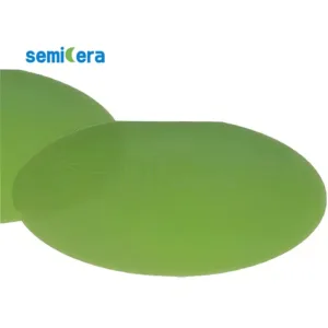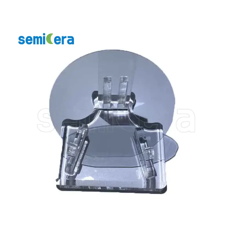
Semicera is excited to offer 2″ Gallium Oxide Substrates, a cutting-edge material designed to enhance the performance of advanced semiconductor devices. These substrates, made from Gallium Oxide (Ga2O3), feature an ultra-wide bandgap, making them an ideal choice for high-power, high-frequency, and UV optoelectronic applications.
Principais recursos:
• Ultra-Wide Bandgap: O 2″ Gallium Oxide Substrates provide an outstanding bandgap of approximately 4.8 eV, allowing for higher voltage and temperature operation, far exceeding the capabilities of traditional semiconductor materials like silicon.
• Exceptional Breakdown Voltage: These substrates enable devices to handle significantly higher voltages, making them perfect for power electronics, especially in high-voltage applications.
• Excellent Thermal Conductivity: With superior thermal stability, these substrates maintain consistent performance even in extreme thermal environments, ideal for high-power and high-temperature applications.
• High-Quality Material: O 2″ Gallium Oxide Substrates offer low defect densities and high crystalline quality, ensuring the reliable and efficient performance of your semiconductor devices.
• Versatile Applications: These substrates are suited for a range of applications, including power transistors, Schottky diodes, and UV-C LED devices, offering a robust foundation for both power and optoelectronic innovations.
Unlock the full potential of your semiconductor devices with Semicera’s 2″ Gallium Oxide Substrates. Our substrates are designed to meet the demanding needs of today’s advanced applications, ensuring high performance, reliability, and efficiency. Choose Semicera for state-of-the-art semiconductor materials that drive innovation.
|
Unid |
Produção |
Pesquisar |
Fictício |
|
Parâmetros de cristal |
|||
|
Polytype |
4H |
||
|
Erro de orientação da superfície |
4±0.15° |
||
|
Parâmetros elétricos |
|||
|
Dopante |
nitrogênio do tipo n |
||
|
Resistividade |
0,015-0.025OHM · cm |
||
|
Parâmetros mecânicos |
|||
|
Diâmetro |
150,0 ± 0,2 mm |
||
|
Grossura |
350 ± 25 µm |
||
|
Orientação plana primária |
[1-100]±5° |
||
|
Comprimento plano primário |
47,5 ± 1,5 mm |
||
|
Apartamento secundário |
Nenhum |
||
|
TTV |
≤5 µm |
≤10 µm |
≤15 µm |
|
LTV |
≤3 μm (5mm*5mm) |
≤5 μm (5mm*5mm) |
≤10 μm (5mm*5mm) |
|
Arco |
-15μm ~ 15μm |
-35μm ~ 35μm |
-45μm ~ 45μm |
|
Urdidura |
≤35 µm |
≤45 µm |
≤55 µm |
|
A rugosidade frontal (Si-face) (AFM) |
Ra≤0,2 nm (5μm*5μm) |
||
|
Estrutura |
|||
|
Densidade de micropipe |
<1 ea/cm2 |
<10 ea/cm2 |
<15 ea/cm2 |
|
Impurezas de metal |
≤5E10atoms/cm2 |
N / D |
|
|
Bpd |
≤1500 ea/cm2 |
≤3000 ea/cm2 |
N / D |
|
TSD |
≤500 ea/cm2 |
≤1000 ea/cm2 |
N / D |
|
Qualidade frontal |
|||
|
Frente |
Si |
||
|
Acabamento superficial |
Si-face cmp |
||
|
Partículas |
≤60ea/wafer (size≥0,3μm) |
N / D |
|
|
Arranhões |
≤5ea/mm. Comprimento cumulativo ≤DIAMETER |
Comprimento cumulativo ≤2*diâmetro |
N / D |
|
Casca de laranja/poços/manchas/estrias/rachaduras/contaminação |
Nenhum |
N / D |
|
|
Chips/recuos/fraturas/placas de fratura/placas hexadecimais |
Nenhum |
||
|
Áreas de poliateiro |
Nenhum |
Área cumulativa ≤20% |
Área cumulativa ≤30% |
|
Marcada a laser dianteira |
Nenhum |
||
|
Qualidade de volta |
|||
|
Final traseiro |
CMP C-FACE |
||
|
Arranhões |
≤5ea/mm, comprimento cumulativo≤2*diâmetro |
N / D |
|
|
Defeitos traseiros (chips/recuos de borda) |
Nenhum |
||
|
Rugosidade de volta |
Ra≤0,2 nm (5μm*5μm) |
||
|
Marcação de laser traseiro |
1 mm (da borda superior) |
||
|
Borda |
|||
|
Borda |
Chanfro |
||
|
Embalagem |
|||
|
Embalagem |
Epi pronto com embalagem a vácuo Embalagem de cassetes de várias linhas |
||
|
*Notas : “NA” significa que nenhum item de solicitação não mencionado pode se referir ao Semi-STD. |
|||