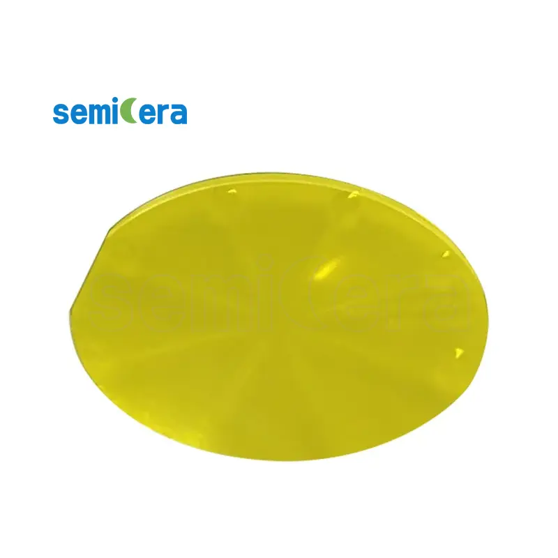
Semicera 3C-SiC Wafer Substrates are engineered to provide a robust platform for next-generation power electronics and high-frequency devices. With superior thermal properties and electrical characteristics, these substrates are designed to meet the demanding requirements of modern technology.
The 3C-SiC (Cubic Silicon Carbide) structure of Semicera Wafer Substrates offers unique advantages, including higher thermal conductivity and a lower thermal expansion coefficient compared to other semiconductor materials. This makes them an excellent choice for devices operating under extreme temperatures and high-power conditions.
With a high electrical breakdown voltage and superior chemical stability, Semicera 3C-SiC Wafer Substrates ensure long-lasting performance and reliability. These properties are critical for applications such as high-frequency radar, solid-state lighting, and power inverters, where efficiency and durability are paramount.
Semicera’s commitment to quality is reflected in the meticulous manufacturing process of their 3C-SiC Wafer Substrates, ensuring uniformity and consistency across every batch. This precision contributes to the overall performance and longevity of the electronic devices built upon them.
By choosing Semicera 3C-SiC Wafer Substrates, manufacturers gain access to a cutting-edge material that enables the development of smaller, faster, and more efficient electronic components. Semicera continues to support technological innovation by providing reliable solutions that meet the evolving demands of the semiconductor industry.
|
Unid |
Produção |
Pesquisar |
Fictício |
|
Parâmetros de cristal |
|||
|
Polytype |
4H |
||
|
Erro de orientação da superfície |
4±0.15° |
||
|
Parâmetros elétricos |
|||
|
Dopante |
nitrogênio do tipo n |
||
|
Resistividade |
0,015-0.025OHM · cm |
||
|
Parâmetros mecânicos |
|||
|
Diâmetro |
150,0 ± 0,2 mm |
||
|
Grossura |
350 ± 25 µm |
||
|
Orientação plana primária |
[1-100]±5° |
||
|
Comprimento plano primário |
47,5 ± 1,5 mm |
||
|
Apartamento secundário |
Nenhum |
||
|
TTV |
≤5 µm |
≤10 µm |
≤15 µm |
|
LTV |
≤3 μm (5mm*5mm) |
≤5 μm (5mm*5mm) |
≤10 μm (5mm*5mm) |
|
Arco |
-15μm ~ 15μm |
-35μm ~ 35μm |
-45μm ~ 45μm |
|
Urdidura |
≤35 µm |
≤45 µm |
≤55 µm |
|
A rugosidade frontal (Si-face) (AFM) |
Ra≤0,2 nm (5μm*5μm) |
||
|
Estrutura |
|||
|
Densidade de micropipe |
<1 ea/cm2 |
<10 ea/cm2 |
<15 ea/cm2 |
|
Impurezas de metal |
≤5E10atoms/cm2 |
N / D |
|
|
Bpd |
≤1500 ea/cm2 |
≤3000 ea/cm2 |
N / D |
|
TSD |
≤500 ea/cm2 |
≤1000 ea/cm2 |
N / D |
|
Qualidade frontal |
|||
|
Frente |
Si |
||
|
Acabamento superficial |
Si-face cmp |
||
|
Partículas |
≤60ea/wafer (size≥0,3μm) |
N / D |
|
|
Arranhões |
≤5ea/mm. Comprimento cumulativo ≤DIAMETER |
Comprimento cumulativo ≤2*diâmetro |
N / D |
|
Casca de laranja/poços/manchas/estrias/rachaduras/contaminação |
Nenhum |
N / D |
|
|
Chips/recuos/fraturas/placas de fratura/placas hexadecimais |
Nenhum |
||
|
Áreas de poliateiro |
Nenhum |
Área cumulativa ≤20% |
Área cumulativa ≤30% |
|
Marcada a laser dianteira |
Nenhum |
||
|
Qualidade de volta |
|||
|
Final traseiro |
CMP C-FACE |
||
|
Arranhões |
≤5ea/mm, comprimento cumulativo≤2*diâmetro |
N / D |
|
|
Defeitos traseiros (chips/recuos de borda) |
Nenhum |
||
|
Rugosidade de volta |
Ra≤0,2 nm (5μm*5μm) |
||
|
Marcação de laser traseiro |
1 mm (da borda superior) |
||
|
Borda |
|||
|
Borda |
Chanfro |
||
|
Embalagem |
|||
|
Embalagem |
Epi pronto com embalagem a vácuo Embalagem de cassetes de várias linhas |
||
|
*Notas : “NA” significa que nenhum item de solicitação não mencionado pode se referir ao Semi-STD. |
|||


