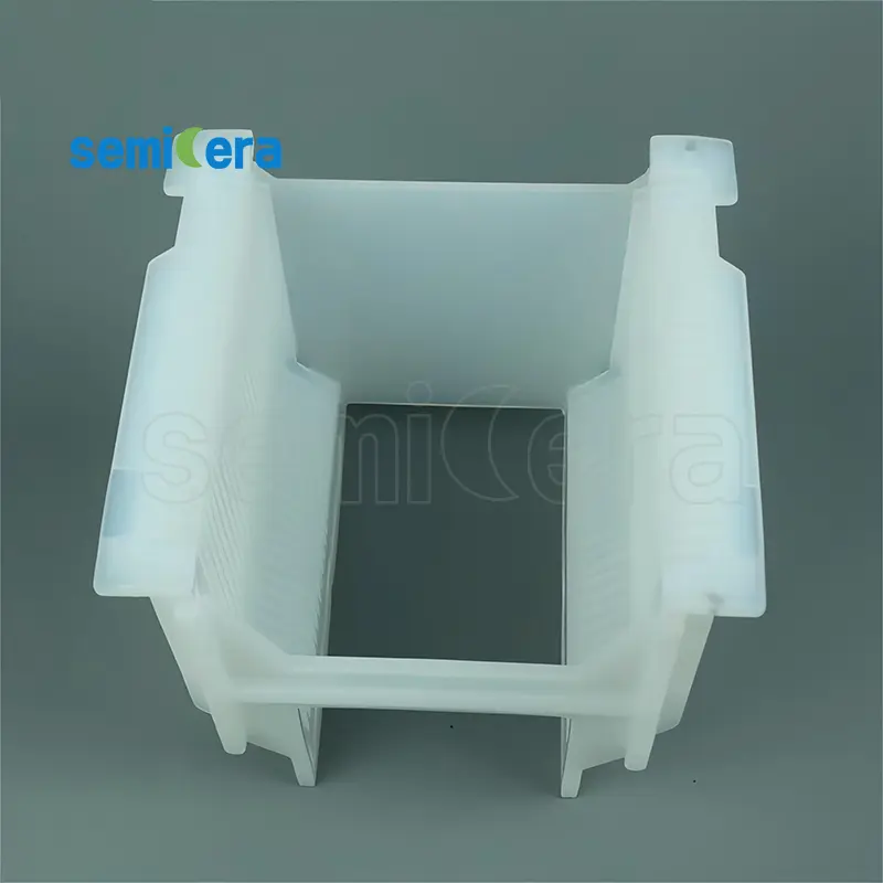
Semicera presents the industry-leading Portadores de wafer, engineered to provide superior protection and seamless transportation of delicate semiconductor wafers across various stages of the manufacturing process. Our Portadores de wafer are meticulously designed to meet the stringent demands of modern semiconductor fabrication, ensuring the integrity and quality of your wafers are maintained at all times.
Principais recursos:
• Premium Material Construction: Crafted from high-quality, contamination-resistant materials that guarantee durability and longevity, making them ideal for cleanroom environments.
• Precision Design: Features precise slot alignment and secure holding mechanisms to prevent wafer slippage and damage during handling and transportation.
• Versatile Compatibility: Accommodates a wide range of wafer sizes and thicknesses, providing flexibility for various semiconductor applications.
• Ergonomic Handling: Lightweight and user-friendly design facilitates easy loading and unloading, enhancing operational efficiency and reducing handling time.
• Customizable Options: Offers customization to meet specific requirements, including material choice, size adjustments, and labeling for optimized workflow integration.
Enhance your semiconductor manufacturing process with Semicera’s Portadores de wafer, the perfect solution for safeguarding your wafers against contamination and mechanical damage. Trust in our commitment to quality and innovation to deliver products that not only meet but exceed industry standards, ensuring your operations run smoothly and efficiently.
|
Unid |
Produção |
Pesquisar |
Fictício |
|
Parâmetros de cristal |
|||
|
Polytype |
4H |
||
|
Erro de orientação da superfície |
4±0.15° |
||
|
Parâmetros elétricos |
|||
|
Dopante |
nitrogênio do tipo n |
||
|
Resistividade |
0,015-0.025OHM · cm |
||
|
Parâmetros mecânicos |
|||
|
Diâmetro |
150,0 ± 0,2 mm |
||
|
Grossura |
350 ± 25 µm |
||
|
Orientação plana primária |
[1-100]±5° |
||
|
Comprimento plano primário |
47,5 ± 1,5 mm |
||
|
Apartamento secundário |
Nenhum |
||
|
TTV |
≤5 µm |
≤10 µm |
≤15 µm |
|
LTV |
≤3 μm (5mm*5mm) |
≤5 μm (5mm*5mm) |
≤10 μm (5mm*5mm) |
|
Arco |
-15μm ~ 15μm |
-35μm ~ 35μm |
-45μm ~ 45μm |
|
Urdidura |
≤35 µm |
≤45 µm |
≤55 µm |
|
A rugosidade frontal (Si-face) (AFM) |
Ra≤0,2 nm (5μm*5μm) |
||
|
Estrutura |
|||
|
Densidade de micropipe |
<1 ea/cm2 |
<10 ea/cm2 |
<15 ea/cm2 |
|
Impurezas de metal |
≤5E10atoms/cm2 |
N / D |
|
|
Bpd |
≤1500 ea/cm2 |
≤3000 ea/cm2 |
N / D |
|
TSD |
≤500 ea/cm2 |
≤1000 ea/cm2 |
N / D |
|
Qualidade frontal |
|||
|
Frente |
Si |
||
|
Acabamento superficial |
Si-face cmp |
||
|
Partículas |
≤60ea/wafer (size≥0,3μm) |
N / D |
|
|
Arranhões |
≤5ea/mm. Comprimento cumulativo ≤DIAMETER |
Comprimento cumulativo ≤2*diâmetro |
N / D |
|
Casca de laranja/poços/manchas/estrias/rachaduras/contaminação |
Nenhum |
N / D |
|
|
Chips/recuos/fraturas/placas de fratura/placas hexadecimais |
Nenhum |
||
|
Áreas de poliateiro |
Nenhum |
Área cumulativa ≤20% |
Área cumulativa ≤30% |
|
Marcada a laser dianteira |
Nenhum |
||
|
Qualidade de volta |
|||
|
Final traseiro |
CMP C-FACE |
||
|
Arranhões |
≤5ea/mm, comprimento cumulativo≤2*diâmetro |
N / D |
|
|
Defeitos traseiros (chips/recuos de borda) |
Nenhum |
||
|
Rugosidade de volta |
Ra≤0,2 nm (5μm*5μm) |
||
|
Marcação de laser traseiro |
1 mm (da borda superior) |
||
|
Borda |
|||
|
Borda |
Chanfro |
||
|
Embalagem |
|||
|
Embalagem |
Epi pronto com embalagem a vácuo Embalagem de cassetes de várias linhas |
||
|
*Notas : “NA” significa que nenhum item de solicitação não mencionado pode se referir ao Semi-STD. |
|||


