High-purity SiC Crystal Growth demands careful attention to several factors.
- Source material purity determines the final crystal’s electrical properties.
- Particle size and distribution affect the uniformity of crystal formation.
- Temperature gradient control prevents unwanted defects.
- Process optimization influences yield and quality, especially in china SiC Crystal Growth.
SiC Single Crystal Growth Technology enables advanced devices to meet strict reliability standards.
Key Takeaways
- High-purity raw materials with uniform particle size are essential to produce defect-free SiC crystals that improve device performance and lifespan.
- Precise control of temperature gradients and a clean growth environment prevent defects and ensure the formation of high-quality crystals.
- Choosing the right crystal growth method and carefully managing pressure and gas flow optimize purity and reduce production costs.
- Regular defect detection and impurity measurement help maintain quality and guide improvements in the crystal growth process.
- Continuous monitoring and process optimization lead to better crystals, higher yields, and more reliable advanced electronic devices.
Significance of High-Purity SiC Crystal Growth in Advanced Technologies
Requirements for Power Electronics and Quantum Devices
High-purity silicon carbide crystals play a vital role in modern technology. Power electronics need materials that can handle high voltages and temperatures. Devices such as MOSFETs and Schottky diodes use these crystals to improve efficiency and reduce energy loss. Quantum devices also depend on pure crystals. These devices require a stable and defect-free environment to maintain quantum states. Even a small impurity can disrupt performance.
Note: Engineers select high-purity SiC crystals to ensure reliable operation in demanding environments.
A table below shows the main requirements for these applications:
| Application | Key Requirement | Benefit |
|---|---|---|
| Power Electronics | High breakdown voltage | Handles high power loads |
| Quantum Devices | Low defect density | Stable quantum operations |
Influence on Device Performance and Longevity
The quality of the crystal directly affects device performance. Fewer defects mean better electrical properties. Devices last longer when the crystal has fewer impurities. High-purity crystals help prevent early device failure. They also allow for higher operating temperatures and faster switching speeds.
- Devices with pure crystals show:
- Lower energy loss
- Higher reliability
- Longer service life
Manufacturers monitor purity at every step. They use advanced tools to detect and remove defects. This careful process ensures that each device meets strict industry standards.
Source Material Selection and Preparation in SiC Crystal Growth

Raw Material Purity and Its Impact
Raw material purity stands as a critical factor in SiC Crystal Growth. High-purity silicon and carbon sources help reduce unwanted impurities in the final crystal. These impurities can introduce defects, lower electrical performance, and shorten device lifespan. Manufacturers often select materials with purity levels above 99.999%. This level of purity ensures that the grown crystals meet the strict requirements of advanced applications.
Note: Even trace amounts of metals or oxygen can cause significant problems in the crystal structure.
A comparison table below highlights the effects of different purity levels:
| Purity Level | Defect Rate | Electrical Performance | Application Suitability |
|---|---|---|---|
| 99.9% | High | Poor | Limited |
| 99.99% | Moderate | Good | Standard |
| 99.999% and above | Low | Excellent | Advanced (Power, Quantum) |
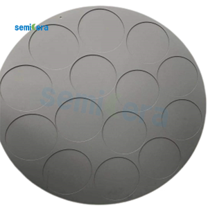
Particle Size, Distribution, and Pre-Treatment
Particle size and distribution also play a major role in crystal growth. Uniform particle size helps create a consistent growth environment. Large particles may not react completely, while very fine particles can cause agglomeration. Both situations can lead to defects in the crystal.
Manufacturers often use the following steps to prepare raw materials:
- Sieve the powder to achieve uniform particle size.
- Wash the particles to remove surface contaminants.
- Dry the material under controlled conditions.
Pre-treatment steps help remove unwanted residues and moisture. This preparation reduces the risk of introducing new impurities during SiC Crystal Growth. Consistent particle size and clean surfaces support the formation of high-quality crystals.
Temperature Gradient and Growth Environment Control in SiC Crystal Growth
Temperature Uniformity and Gradient Optimization
Precise temperature control shapes the quality of SiC crystals. Engineers set a stable temperature gradient to guide crystal growth. A uniform gradient helps atoms arrange in an orderly way. This process reduces the risk of cracks and unwanted polytypes. If the temperature changes too quickly, defects may form in the crystal. Operators use advanced sensors to monitor the furnace. They adjust the heat source to keep the temperature steady.
Tip: Consistent temperature gradients lead to larger, defect-free SiC crystals.
Atmosphere Control and Contamination Prevention
The growth environment must stay clean. Engineers fill the furnace with inert gases like argon. These gases prevent unwanted reactions with the crystal. Even a small amount of oxygen or moisture can introduce defects. Operators use gas purifiers and leak detectors to keep the atmosphere pure. They also monitor gas flow rates to avoid turbulence. Clean environments help maintain the high purity needed for advanced devices.
A simple checklist for atmosphere control:
- Use high-purity inert gases
- Check for leaks before starting
- Monitor gas flow and pressure
- Replace filters and purifiers regularly
Crucible and Furnace Material Considerations
The choice of crucible and furnace materials affects SiC Crystal Growth. Engineers select materials that do not react with silicon carbide at high temperatures. Graphite crucibles are common because they resist chemical attack. The furnace lining must also withstand high heat and avoid releasing impurities. Regular inspection of these materials prevents contamination.
A table below shows common materials and their properties:
| Material | Heat Resistance | Chemical Stability | Suitability |
|---|---|---|---|
| Graphite | Excellent | High | Preferred |
| Quartz | Moderate | Low | Not Recommended |
| Alumina | Good | Moderate | Sometimes Used |
Careful selection and maintenance of furnace components support the production of high-purity crystals.
Process Parameters and Equipment Configuration for SiC Crystal Growth
Growth Method Selection: PVT, HTCVD, and Top-Seeded Solution Growth
Engineers select the right growth method based on the desired crystal quality and application. Physical Vapor Transport (PVT) stands as the most common technique for producing large SiC crystals. In this method, silicon carbide powder vaporizes at high temperatures and then condenses on a cooler seed crystal. This process creates high-purity, bulk crystals suitable for power electronics.
High-Temperature Chemical Vapor Deposition (HTCVD) offers another approach. This method uses gas-phase chemicals that react at elevated temperatures to form SiC layers on a substrate. HTCVD produces crystals with fewer impurities and better control over thickness. Researchers often use this method for specialized applications that require thin, high-quality layers.
Top-Seeded Solution Growth (TSSG) involves dissolving silicon and carbon in a molten metal solvent. A seed crystal sits at the top and slowly pulls the SiC from the solution. TSSG allows for precise control over crystal structure and reduces the risk of unwanted polytypes. Each method presents unique advantages and challenges. The choice depends on the target application, required purity, and available equipment.
Tip: Selecting the right growth method can improve yield and reduce production costs.
Pressure, Gas Flow, and Real-Time Monitoring
Precise control of pressure and gas flow shapes the outcome of SiC Crystal Growth. Operators adjust the pressure inside the furnace to influence the rate of crystal formation. Low pressure can help reduce unwanted defects, while high pressure may speed up growth but increase the risk of imperfections.
Gas flow also plays a key role. Engineers use high-purity gases like argon or hydrogen to create a stable environment. They regulate the flow rate to ensure even distribution around the growing crystal. Uneven gas flow can cause temperature fluctuations and introduce defects.
Real-time monitoring systems track temperature, pressure, and gas composition during the process. Sensors provide instant feedback, allowing operators to make quick adjustments. This technology helps maintain optimal conditions and prevents contamination. Modern equipment often includes automated controls for greater accuracy and repeatability.
A table below summarizes key parameters and their effects:
| Parameter | Effect on Crystal Growth | Control Method |
|---|---|---|
| Pressure | Defect density, growth rate | Vacuum pumps, gauges |
| Gas Flow | Purity, uniformity | Mass flow controllers |
| Temperature | Crystal structure, size | Thermocouples, heaters |
Techniques for Defect Minimization and Polytype Control
Defect minimization stands as a top priority in SiC crystal production. Engineers use several techniques to achieve this goal. Careful control of temperature gradients helps prevent the formation of cracks and stacking faults. Uniform heating ensures that atoms arrange in the correct order.
Polytype control is also important. SiC can form different crystal structures, called polytypes, which affect electrical properties. Operators adjust growth conditions, such as temperature and gas composition, to favor the desired polytype. They may also use specially oriented seed crystals to guide the structure.
Advanced inspection tools, like X-ray diffraction and optical microscopy, help detect defects early. Feedback from these tools allows for process adjustments in future growth cycles. Continuous improvement leads to higher yields and better device performance.
Note: Consistent monitoring and process optimization reduce defects and ensure the right polytype for advanced applications.
Post-Growth Characterization and Quality Assessment in SiC Crystal Growth

Defect Detection and Dislocation Analysis
Engineers use advanced tools to find defects in SiC crystals. They often rely on X-ray topography and optical microscopy. These methods help them see cracks, stacking faults, and dislocations. Dislocations can lower the performance of electronic devices. Companies want to keep the number of these defects as low as possible. They also use etching techniques to make hidden defects visible. Early detection helps prevent faulty crystals from reaching the next stage.
Tip: Regular defect analysis ensures that only high-quality crystals move forward in the production process.
Impurity Profiling and Measurement
Impurities can change the electrical properties of SiC crystals. Scientists use methods like Secondary Ion Mass Spectrometry (SIMS) and Glow Discharge Mass Spectrometry (GDMS) to measure impurity levels. These tools can detect even tiny amounts of unwanted elements. Accurate impurity profiling helps companies meet strict industry standards. They compare results to target values to ensure the crystals are pure enough for advanced uses.
A table below shows common impurities and their effects:
| Impurity | Effect on Crystal |
|---|---|
| Oxygen | Reduces conductivity |
| Nitrogen | Alters carrier density |
| Metals | Causes device failure |
Feedback Mechanisms for Process Improvement
Quality assessment does not end with measurement. Engineers use the data from defect and impurity analysis to improve SiC Crystal Growth. They adjust process parameters based on feedback. This cycle helps reduce defects and impurities in future batches. Teams often hold review meetings to discuss results and plan changes. Continuous feedback leads to better crystals and more reliable devices.
Note: Ongoing process improvement is key to staying competitive in the SiC industry.
Achieving high-purity crystals demands strict attention to every step. Engineers select the best materials and control temperature with precision. They monitor each process to reduce defects and improve quality. Careful post-growth checks help ensure only the best crystals reach advanced devices. Teams who follow best practices see better results and longer device life. Continuous improvement and strong quality control help meet the needs of modern technology.
FAQ
What makes high-purity SiC crystals important for electronics?
High-purity SiC crystals help devices work better and last longer. They reduce energy loss and prevent early failure. Engineers use these crystals in power electronics and quantum devices for better performance.
How do engineers check for defects in SiC crystals?
Engineers use tools like X-ray topography and optical microscopes. These tools help them find cracks, stacking faults, and dislocations. Early detection keeps only the best crystals for advanced devices.
Which growth method produces the purest SiC crystals?
| Growth Method | Purity Level | Common Use |
|---|---|---|
| PVT | High | Power electronics |
| HTCVD | Very High | Quantum devices |
| TSSG | High | Research |
HTCVD often gives the purest crystals.
Can small impurities affect SiC crystal performance?
Even tiny amounts of metals or oxygen can change how a crystal works. These impurities may lower conductivity or cause device failure. Engineers always aim for the lowest impurity levels.