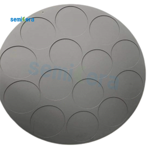
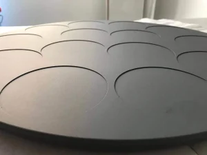
Silicon-On-Insulator (SOI) Wafer technology delivers faster chip speeds and lower energy use in 2025. Engineers use a Silicon coating over an insulating layer to boost performance. SOI Wafers help devices run cooler and last longer. The Silicon On Insulator Wafer design supports smaller, more efficient electronics.
Devices built with this technology set new standards for reliability and innovation.
Key Takeaways
- SOI wafers use a special layered design that reduces power loss and heat, making chips faster and more efficient.
- This technology helps devices run cooler, last longer, and perform better in areas like mobile phones, cars, and data centers.
- SOI wafers improve chip reliability by protecting against electrical failures and heat damage, which is vital for critical systems.
- Though SOI wafers cost more to produce and require new manufacturing steps, their benefits in speed and energy savings are worth it.
- Ongoing research and wider adoption of SOI technology promise even better chip performance and more advanced electronics in the future.
Silicon-On-Insulator (SOI) Wafer Structure and Function
How SOI Wafers Work
A Silicon-On-Insulator (SOI) Wafer uses a special layered structure. Engineers place a thin layer of silicon on top of an insulating material, usually silicon dioxide. This design separates the active silicon layer from the bulk substrate below. The insulating layer blocks unwanted electrical currents. As a result, chips built on SOI wafers show less leakage and better control of electrical signals.
The process starts with a base silicon wafer. Manufacturers add a buried oxide layer, then bond a thin silicon film on top. This top layer forms the area where transistors and circuits operate. The buried oxide acts as a barrier, which helps devices run cooler and use less power.
Note: The insulating layer in SOI wafers plays a key role in reducing energy loss and improving chip performance.
Differences from Bulk Silicon
SOI wafers differ from traditional bulk silicon in several ways. Bulk silicon uses a single, thick layer of silicon without an insulating barrier. This structure allows more electrical current to flow through the chip, which can cause higher power use and more heat.
Key differences include:
- Structure: SOI wafers have three layers—top silicon, buried oxide, and base silicon. Bulk silicon has only one thick silicon layer.
- Performance: SOI wafers reduce electrical leakage and improve speed. Bulk silicon chips often lose more energy as heat.
- Size: SOI technology supports smaller, more compact chips. Bulk silicon limits how small devices can get.
A simple table highlights these contrasts:
| Feature | SOI Wafer | Bulk Silicon |
|---|---|---|
| Layers | 3 (Silicon/Oxide/Silicon) | 1 (Silicon) |
| Power Loss | Low | High |
| Heat Generation | Low | High |
| Device Size | Smaller | Larger |
Performance Advantages of Silicon-On-Insulator (SOI) Wafer Technology
Reduced Power Consumption
Engineers choose Silicon-On-Insulator (SOI) Wafer technology to lower the power needs of modern chips. The insulating layer inside each wafer blocks stray electrical currents. This design stops energy from leaking away. Devices built on SOI wafers use less electricity than those made with bulk silicon. Lower power use means longer battery life for phones, tablets, and laptops. It also helps companies build greener data centers.
Tip: Lower power consumption not only saves energy but also reduces heat, which protects sensitive chip parts.
Increased Speed and Efficiency
SOI wafers help chips run faster. The thin silicon layer on top of the insulator allows signals to move quickly. Less interference from stray currents means each transistor can switch on and off at higher speeds. This leads to better performance in everything from gaming consoles to high-speed servers.
Key benefits include:
- Faster data processing
- Shorter response times
- Improved multitasking
A simple table shows the impact:
| Feature | Bulk Silicon | SOI Wafer |
|---|---|---|
| Signal Speed | Moderate | High |
| Switching Delay | Longer | Shorter |
| Processing Power | Standard | Enhanced |
Superior Thermal Management
Heat can damage chips and slow down devices. SOI wafers solve this problem by using an insulating layer that keeps heat from spreading. The buried oxide layer acts as a barrier, so less heat reaches the rest of the chip. This design keeps devices cooler, even when they work hard for long hours.
- Cooler chips last longer.
- Devices can run at higher speeds without overheating.
- Less need for bulky cooling systems.
Note: Good thermal management helps prevent system crashes and extends the life of electronics.
Enhanced Device Reliability
Device reliability stands as a top priority for chip designers in 2025. The Silicon-On-Insulator (SOI) Wafer structure helps engineers build chips that resist common failures. The buried oxide layer acts as a shield, blocking unwanted electrical currents. This barrier reduces the risk of short circuits and electrical noise. Chips built on SOI wafers show fewer defects over time.
Many devices face problems from heat, voltage spikes, and radiation. SOI wafers protect sensitive circuits from these threats. The insulating layer keeps heat from spreading, which lowers the chance of overheating. Devices can run for longer periods without breaking down. This feature proves vital in mission-critical systems, such as medical devices and automotive safety controls.
Note: Reliable chips mean fewer repairs and less downtime for users.
Engineers also see fewer latch-up events with SOI technology. Latch-up can cause chips to fail suddenly. The insulating layer in SOI wafers blocks the paths that lead to latch-up. This protection increases the lifespan of each chip.
A quick look at the benefits:
- Lower risk of electrical failure
- Better resistance to heat and voltage stress
- Fewer defects and longer device life
- Improved safety for critical applications
A table highlights the reliability improvements:
| Reliability Factor | Bulk Silicon | SOI Wafer |
|---|---|---|
| Latch-Up Risk | High | Low |
| Heat Resistance | Moderate | High |
| Defect Rate | Higher | Lower |
| Lifespan | Shorter | Longer |
Engineers trust SOI wafers for devices that must work every time. This technology sets a new standard for chip reliability in modern electronics.
Applications of Silicon-On-Insulator (SOI) Wafer Solutions in 2025
Consumer Electronics and Mobile Devices
Manufacturers use Silicon-On-Insulator (SOI) Wafer technology to build faster and more reliable smartphones, tablets, and wearables. Devices with SOI wafers show longer battery life and better heat control. Users notice that their phones stay cool, even during heavy gaming or video streaming. SOI wafers also help engineers design thinner and lighter products. This technology supports high-resolution displays and advanced camera features.
- Longer battery life for mobile devices
- Thinner and lighter designs
- Improved performance for gaming and streaming
Note: SOI wafers help mobile devices run demanding apps without overheating.
Automotive and Autonomous Systems
Automotive companies rely on SOI wafer solutions for safety and performance. Cars with advanced driver-assistance systems (ADAS) need chips that work in extreme temperatures. SOI wafers provide strong resistance to heat and electrical noise. This makes them ideal for sensors, cameras, and control units in electric and self-driving vehicles. Engineers trust SOI wafers to deliver reliable operation in harsh environments.
A table shows key benefits for automotive use:
| Feature | Benefit |
|---|---|
| Heat Resistance | Stable in hot climates |
| Electrical Isolation | Fewer system errors |
| Reliability | Safer driving experience |
Data Centers and High-Performance Computing
Data centers demand chips that process information quickly and use less energy. SOI wafer technology helps servers handle large workloads without overheating. Companies use these wafers to build processors that support cloud computing, artificial intelligence, and big data analytics. The improved thermal management reduces the need for expensive cooling systems. This leads to lower operating costs and more efficient data centers.
- Faster data processing
- Lower power consumption
- Reduced cooling requirements
Tip: SOI wafers help data centers run more efficiently and support the growth of digital services.
AI, IoT, and 5G Technologies
Artificial intelligence (AI), the Internet of Things (IoT), and 5G networks drive the demand for faster and more reliable chips in 2025. These technologies require processors that handle large amounts of data with low delay. Engineers use advanced wafer solutions to meet these needs.
AI systems process complex tasks like image recognition and language translation. They need chips that deliver high speed and efficiency. SOI wafers help AI chips run faster and use less power. This allows smart assistants and robots to respond quickly and learn from new data.
IoT devices connect everyday objects to the internet. Smart home sensors, wearable health trackers, and industrial machines all rely on tiny, energy-efficient chips. SOI wafer technology supports the miniaturization of these devices. It also helps them last longer on a single battery charge.
5G networks promise fast wireless connections for phones, cars, and smart cities. Chips in 5G devices must handle high frequencies and avoid signal loss. SOI wafers provide strong electrical isolation, which reduces interference. This leads to clearer calls, faster downloads, and more stable connections.
A table shows how these technologies benefit from SOI wafer solutions:
| Technology | Key Benefit | Result |
|---|---|---|
| AI | High speed, low power | Faster learning, quick response |
| IoT | Small size, efficiency | Longer battery life, more connections |
| 5G | Signal isolation | Reliable, high-speed data |
Note: SOI wafer technology supports the growth of smart devices and networks by improving chip performance and reliability.
Challenges and Limitations of Silicon-On-Insulator (SOI) Wafer Technology
Manufacturing Complexity and Cost
Chip makers face several hurdles when producing these advanced wafers. The process requires special equipment and extra steps compared to regular silicon wafers. Engineers must carefully bond thin layers and control the thickness of each part. This precision increases the risk of defects during manufacturing. As a result, the cost per wafer rises. Many companies find it hard to balance high performance with affordable prices.
- Specialized tools increase production costs.
- Extra quality checks slow down output.
- Higher risk of defects leads to more waste.
Note: Companies often pass these higher costs to customers, making devices more expensive.
Integration with Existing Technologies
Many factories still use older systems designed for bulk silicon chips. Switching to new wafer types can cause problems. Engineers must redesign circuits and update software to match the new structure. Some tools and machines may not work with the new wafers. This slows down the adoption of the technology.
A table shows common integration issues:
| Challenge | Impact |
|---|---|
| Circuit Redesign | Longer development time |
| Tool Compatibility | Extra investment needed |
| Software Adjustments | More testing required |
Supply Chain and Scalability
Suppliers must deliver high-quality wafers in large numbers. Not all regions have the right materials or skilled workers. Delays in shipping or shortages of parts can stop production. Companies may struggle to scale up quickly when demand rises.
- Limited suppliers create bottlenecks.
- Shipping delays affect delivery times.
- Shortages can halt manufacturing.
Tip: Building a strong supply chain helps companies avoid these problems and meet market needs.
Future Trends in Silicon-On-Insulator (SOI) Wafer Innovation
Advances in Materials and Processes
Engineers continue to improve the materials used in chip manufacturing. They explore new insulators and silicon layers to boost chip performance. Some teams test ultra-thin oxide layers to reduce energy loss. Others use advanced bonding techniques to create smoother surfaces. These changes help chips run faster and last longer.
A few companies now use new chemical processes. These processes make the layers more uniform. Uniform layers mean fewer defects and better yields. Some researchers also study new ways to recycle materials. This step lowers costs and reduces waste.
Tip: Better materials and processes help make chips more reliable and efficient.
Expanding Industry Adoption
More industries now use Silicon-On-Insulator (SOI) Wafer technology. Consumer electronics, automotive, and medical device makers all see the benefits. They choose SOI wafers for their low power use and high reliability. Even small companies can now access this technology.
A table shows how different sectors use SOI wafers:
| Industry | Main Benefit |
|---|---|
| Consumer Tech | Longer battery life |
| Automotive | Heat resistance |
| Medical Devices | High reliability |
Many companies invest in new factories. They want to meet the growing demand for advanced chips. This trend helps lower costs and makes SOI wafers more common.
Research and Collaboration
Universities and tech firms work together to solve tough problems. They share data and test new ideas. Some groups focus on making chips even smaller. Others look for ways to speed up production.
- Joint research speeds up innovation.
- Shared labs help teams test new designs.
- Open data lets more people join the effort.
Note: Collaboration leads to faster progress and better results for everyone.
Silicon-On-Insulator (SOI) Wafer technology leads the way in chip innovation. Engineers see unmatched performance, efficiency, and reliability in new devices. As more companies adopt this solution, the future of electronics and computing looks bright.
Ongoing research and teamwork will unlock even greater potential for this technology in the coming years.
FAQ
What makes SOI wafers different from regular silicon wafers?
SOI wafers use a thin silicon layer on top of an insulator. This design blocks unwanted electrical currents. Regular silicon wafers do not have this insulating layer. SOI wafers help chips run faster and use less power.
Are SOI wafers more expensive to produce?
Yes, SOI wafers cost more to make. The process needs special equipment and extra steps. Manufacturers must control each layer carefully. This increases production costs compared to regular silicon wafers.
Which industries benefit most from SOI wafer technology?
Many industries use SOI wafers. Consumer electronics, automotive, and data centers see the biggest gains. These sectors need chips that run fast, stay cool, and last longer.
Tip: Medical devices and 5G networks also benefit from SOI wafer reliability.
Can SOI wafers help reduce device overheating?
SOI wafers improve thermal management. The insulating layer keeps heat from spreading inside the chip. Devices stay cooler, even during heavy use. This helps prevent overheating and extends device life.