
What are the differences in AlN growth on silicon wafers using different deposition processes?
Written by Lucy@ Semicera.
In semiconductor manufacturing, aluminum nitride (AlN) is an indispensable functional thin-film material. It possesses outstanding comprehensive properties: ultra-high thermal conductivity, excellent electrical insulation, a wide bandgap of roughly 6.2 eV, high breakdown voltage, and outstanding thermal and chemical stability. Thanks to these merits, AlN is widely adopted in GaN-based light-emitting diodes (LEDs), high-power power electronic devices, radio frequency acoustic wave filters (SAW/BAW), micro-electro-mechanical systems (MEMS), and deep ultraviolet photodetectors.
AlN cannot spontaneously form on silicon (Si) wafers naturally. Manufacturers rely on specialized thin-film deposition technologies to grow uniform AlN films on silicon substrates. Different deposition methods differ drastically in reaction mechanisms, required process conditions, crystal film quality, performance limitations, and target industrial applications. This article focuses on the four mainstream industrial and research-grade AlN deposition technologies: MOCVD, PVD magnetron sputtering, ALD, and HVPE, elaborating on their core distinctions and practical characteristics.
Why Grow AlN on Silicon Wafers?
Given the availability of alternative substrates like sapphire and silicon carbide (SiC), silicon wafers remain a mainstream base for AlN growth for three core reasons:
1. Extremely low manufacturing cost
The silicon wafer industry has matured over decades, mass-producing 4-inch, 6-inch, 8-inch, and 12-inch large-size wafers at a far lower price than sapphire and SiC. Most consumer and industrial semiconductor devices prioritize silicon substrates to cut overall production expenses.
2. AlN acts as a critical strain buffer layer
Direct epitaxy of gallium nitride (GaN) on silicon leads to severe lattice mismatch (around 17%) and mismatched thermal expansion coefficients between GaN and Si. Without an intermediate layer, the GaN film will suffer severe cracking, wafer warpage, high dislocation density, and film peeling during high-temperature growth. AlN serves as a transitional buffer layer between silicon and GaN, effectively relieving lattice strain, reducing defect density, and greatly improving the crystalline quality of subsequent GaN epitaxial layers.
3. Excellent electrical isolation & piezoelectric performance
AlN features ultra-high electrical resistivity. For MEMS and RF acoustic wave devices, AlN can function as insulating isolation layers, piezoelectric functional layers, or dielectric separation layers, which is irreplaceable for high-frequency signal processing and micro-mechanical sensing components.
Four Primary AlN Deposition Technologies
1. MOCVD (Metal-Organic Chemical Vapor Deposition, Industry Standard Mainstream Technology)
Working Principle
Two core precursors—trimethylaluminum (TMA, an aluminum-containing metal-organic source) and ammonia (NH₃, nitrogen source)—are pumped into a sealed reaction chamber. The chamber is heated to 1000–1200 °C, triggering thermal decomposition of the precursor gases. Separated aluminum atoms and nitrogen atoms rearrange atom-by-atom on the silicon wafer surface to form ordered single-crystal AlN, similar to precisely stacking tiny building blocks into a neat regular crystal lattice.
Core Advantages
– Top-tier single-crystal quality: High-temperature epitaxy enables atom-level ordered growth, forming high-quality hexagonal wurtzite single-crystal AlN with minimal crystal defects.
– Low dislocation density: Engineers optimize nucleation layers, multi-step buffer layer structures, and V/III ratio (NH₃/TMAl flow ratio) to mitigate lattice strain between AlN and silicon, drastically cutting dislocation counts.
– Compatible with subsequent GaN epitaxy: MOCVD-grown AlN acts as a perfect template for secondary growth of GaN, AlGaN, and InGaN multi-layer heterostructures.
– Superior thickness uniformity across large wafers; fully mature, standardized mass-production process.
Main Drawbacks
High equipment investment cost, high energy consumption from ultra-high-temperature operation, and relatively moderate film growth speed.
Applications
GaN power devices, GaN LEDs, high-frequency RF epitaxial templates requiring high crystal quality.
2. PVD Magnetron Sputtering (Physical Vapor Deposition)
Working Principle
High-energy plasma bombards a solid pure aluminum target inside a vacuum chamber, knocking aluminum atoms off the target surface. Under a nitrogen-filled atmosphere, free aluminum atoms react with nitrogen ions and deposit onto silicon wafers to form polycrystalline or amorphous AlN films—comparable to blasting aluminum particles onto the substrate surface. Core Advantages
– Low equipment purchase and operation cost; low process temperature ranging from room temperature to 500 °C, compatible with temperature-sensitive silicon-based micro-devices.
– Fast deposition speed for medium-thickness films, easy batch mass production.
Main Drawbacks
Films thicker than several micrometers accumulate massive internal stress, triggering wafer warpage, film cracking, or delamination. The film is mostly polycrystalline without ordered single-crystal lattices, so it cannot support subsequent GaN epitaxial growth.
Typical Applications
MEMS sensors, BAW/SAW radio frequency filters, thin piezoelectric AlN layers for micro-electromechanical chips.
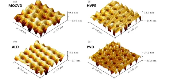
3. ALD (Atomic Layer Deposition)
Working Principle
ALD operates via self-limiting alternating gas pulse cycles, depositing only one atomic layer of material per cycle:
Pulse 1: Inject aluminum precursor gas to allow full adsorption of Al atoms on the wafer surface; purge excess unreacted gas.
Pulse 2: Inject nitrogen precursor to react with adsorbed Al atoms to form a single atomic layer of AlN; purge residual gas again. The two steps repeat thousands of times to accumulate target film thickness.
Core Advantages
– Atomic-level precise thickness control (accuracy up to ~0.1 nm per cycle).
– Exceptional step coverage: Uniformly coats high-aspect-ratio deep trenches, holes, and complex 3D micro-structures without missing coverage.
Main Drawbacks
Extremely slow growth rate: Depositing a 100 nm AlN film requires thousands of repeated cycles, leading to ultra-long production time. It is uneconomical for thick AlN films in mass manufacturing.
Typical Applications
Ultra-thin insulating dielectric layers, conformal passivation layers for advanced micro-nano devices.
4. HVPE (Hydride Vapor Phase Epitaxy)
Working Principle
Aluminum metal reacts with hydrogen chloride gas at high temperature to generate aluminum chloride vapor, which mixes with ammonia gas inside a 1100–1500 °C reaction chamber. Al and N species react and rapidly epitaxially grow thick single-crystal AlN layers on silicon substrates.
Core Advantages
Unmatched ultra-fast growth speed; capable of producing ultra-thick AlN films ranging from tens to hundreds of micrometers, ideal for manufacturing self-supporting AlN single-crystal templates.
Main Drawbacks
Poor thickness uniformity across large wafers, high equipment cost, limited controllability for ultra-thin films, and fewer mature industrial mass-production lines (mostly used in university and corporate research labs).
Typical Applications
Thick free-standing AlN single-crystal templates, laboratory wide-bandgap material research.
|
Comparison Item |
MOCVD |
PVD Magnetron Sputtering |
ALD |
HVPE |
|
Growth Mechanism |
High-temperature epitaxial growth |
Physical sputtering deposition |
Alternating atomic layer self-limiting deposition |
High-temperature hydride epitaxial growth |
|
Overall Crystal Quality |
Highest |
Medium, polycrystalline |
Good, dense polycrystal |
Single-crystal, comparable to MOCVD |
|
Single-Crystal Capability |
Yes (high-quality single crystal) |
No (mostly polycrystalline/amorphous) |
Conditional (rare single crystal under strict tuning) |
Yes (thick single-crystal layers) |
|
Relative Growth Speed |
Medium |
Fast |
Extremely Slow |
Very Fast |
|
Usable Film Thickness Range |
0.1–20 μm |
0.1–10 μm |
Several nm – hundreds of nm |
10–500 μm (ultra-thick films) |
|
Required Process Temperature |
1000–1200 °C |
Room temperature ~ 500 °C |
200–400 °C |
1100–1500 °C |
|
Equipment & Operation Cost |
High |
Low |
Very High |
High |
|
Core Industrial Application Scenarios |
GaN epitaxial substrates, power & optoelectronic devices |
MEMS chips, SAW/BAW RF acoustic filters |
Ultra-thin conformal dielectric isolation layers |
Thick self-supporting AlN templates, laboratory R&D |
Semicera
At Semicera, technological innovation is the core driving force of our development. Our independent internal R&D laboratory continuously optimizes MOCVD and PVD AlN growth technologies through iterative process tuning, multi-dimensional material characterization, and real-device performance verification.
Combining decades of professional semiconductor material expertise and complete experimental testing infrastructure, we have achieved key technical breakthroughs in epitaxial crystal quality, thin-film deposition uniformity, process repeatability, and long-term material reliability. These technical strengths support us in supplying high-performance semiconductor thin-film components and fully customized material growth solutions that meet the strict performance standards of next-generation advanced semiconductor manufacturing.