تشمل مواد أشباه الموصلات الجيل الثالث بشكل أساسي SIC ، GAN ، Diamond ، إلخ ، لأن عرض فجوة النطاق (EG) أكبر من أو يساوي 2.3 فولت الإلكترون (EV) ، والمعروف أيضًا باسم مواد أشباه الموصلات الفجوة على نطاق واسع. مقارنةً بمواد أشباه الموصلات من الجيل الأول والثاني ، فإن مواد أشباه الموصلات الجيل الثالث لها مزايا الموصلية الحرارية العالية ، والجقل الكهربائي العالي ، ومعدل ترحيل الإلكترون المشبع المرتفع ، وارتفاع طاقة الترابط ، والتي يمكن أن تلبي المتطلبات الجديدة للتكنولوجيا الإلكترونية الحديثة لدرجة الحرارة المرتفعة ، والضغط العالي ، وارتفاع التردد ، وظروف الإشعاع وغيرها من الحالات. لديها آفاق تطبيق مهمة في مجالات الدفاع الوطني ، الطيران ، الفضاء ، استكشاف النفط ، التخزين البصري ، وما إلى ذلك ، ويمكن أن تقلل من فقدان الطاقة بأكثر من 50% في العديد من الصناعات الاستراتيجية مثل اتصالات النطاق العريض ، والطاقة الشمسية ، والسيارات المصنعة للتكنولوجيا.
|
Item 项目 |
GaN-FS-C-U-C50 |
GaN-FS-C-N-C50 |
GaN-FS-C-SI-C50 |
|
قطر |
50.8 ± 1 mm |
||
|
سماكة厚度 |
350 ± 25 μm |
||
|
Orientation |
C plane (0001) off angle toward M-axis 0.35 ± 0.15° |
||
|
Prime Flat |
(1-100) 0 ± 0.5°, 16 ± 1 mm |
||
|
شقة ثانوية |
(11-20) 0 ± 3°, 8 ± 1 mm |
||
|
Conductivity |
N-type |
N-type |
Semi-Insulating |
|
Resistivity (300K) |
< 0.1 Ω·cm |
< 0.05 Ω·cm |
> 106 Ω·cm |
|
TTV |
≤ 15 μm |
||
|
BOW |
≤ 20 μm |
||
|
Ga Face Surface Roughness |
< 0.2 nm (polished); |
||
|
or < 0.3 nm (polished and surface treatment for epitaxy) |
|||
|
N Face Surface Roughness |
0.5 ~1.5 μm |
||
|
option: 1~3 nm (fine ground); < 0.2 nm (polished) |
|||
|
Dislocation Density |
From 1 x 10⁵ to 3 x 106 cm-2 (calculated by CL)* |
||
|
Macro Defect Density |
< 2 cm-2 |
||
|
Useable Area |
> 90% (edge and macro defects exclusion) |
||
|
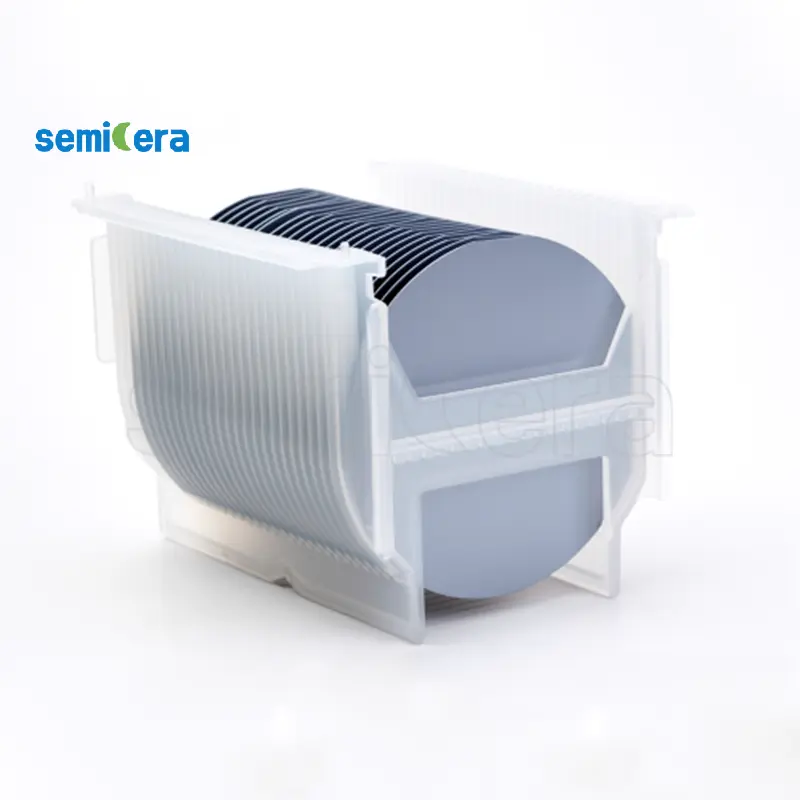
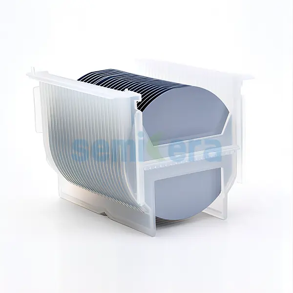
Can be customized according to customer requirements, different structure of silicon, sapphire, SiC based GaN epitaxial sheet. |
|||


