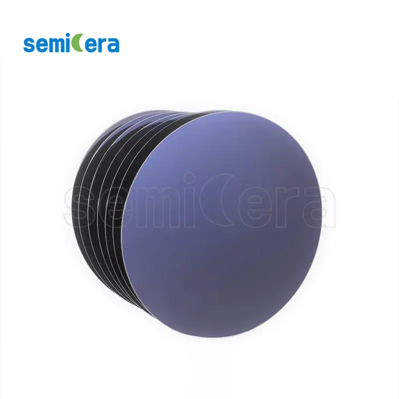
Semicera’s Silicon On Insulator (SOI) Wafer is at the forefront of semiconductor innovation, offering enhanced electrical isolation and superior thermal performance. The SOI structure, consisting of a thin silicon layer on an insulating substrate, provides critical benefits for high-performance electronic devices.
Our SOI wafers are designed to minimize parasitic capacitance and leakage currents, which is essential for developing high-speed and low-power integrated circuits. This advanced technology ensures that devices operate more efficiently, with improved speed and reduced energy consumption, crucial for modern electronics.
The advanced manufacturing processes employed by Semicera guarantee the production of SOI wafers with excellent uniformity and consistency. This quality is vital for applications in telecommunications, automotive, and consumer electronics, where reliable and high-performing components are required.
In addition to their electrical benefits, Semicera’s SOI wafers offer superior thermal insulation, enhancing heat dissipation and stability in high-density and high-power devices. This feature is particularly valuable in applications that involve significant heat generation and require effective thermal management.
By choosing Semicera’s Silicon On Insulator Wafer, you invest in a product that supports the advancement of cutting-edge technologies. Our commitment to quality and innovation ensures that our SOI wafers meet the rigorous demands of today’s semiconductor industry, providing the foundation for next-generation electronic devices.
|
Items |
Productie |
Onderzoek |
Stom |
|
Kristalparameters |
|||
|
Polytype |
4H |
||
|
Oppervlakte -oriëntatiefout |
4±0.15° |
||
|
Elektrische parameters |
|||
|
Dopant |
n-type stikstof |
||
|
Weerstand |
0.015-0.025OHM · cm |
||
|
Mechanische parameters |
|||
|
Diameter |
150,0 ± 0,2 mm |
||
|
Dikte |
350 ± 25 µm |
||
|
Primaire platte oriëntatie |
[1-100]±5° |
||
|
Primaire platte lengte |
47,5 ± 1,5 mm |
||
|
Secundaire flat |
Geen |
||
|
TTV |
≤5 µm |
≤10 µm |
≤15 µm |
|
LTV |
≤3 μm (5 mm*5 mm) |
≤5 μm (5 mm*5 mm) |
≤10 μm (5 mm*5 mm) |
|
Boog |
-15 μm ~ 15 μm |
-35 μm ~ 35 μm |
-45μm ~ 45 urm |
|
Kronkelen |
≤35 µm |
≤45 µm |
≤55 µm |
|
Voorste (si-face) ruwheid (AFM) |
Ra≤0,2 nm (5μm*5μm) |
||
|
Structuur |
|||
|
Micropipe dichtheid |
<1 EA/CM2 |
<10 EA/CM2 |
<15 EA/CM2 |
|
Metaalonzuiverheden |
≤5E10atoms/cm2 |
NA |
|
|
BPD |
≤1500 EA/CM2 |
≤3000 EA/CM2 |
NA |
|
TSD |
≤500 EA/CM2 |
≤1000 EA/CM2 |
NA |
|
Voorste kwaliteit |
|||
|
Voorkant |
Si |
||
|
Oppervlakte -afwerking |
Si-face CMP |
||
|
Deeltjes |
≤60EA/wafer (grootte ≥ 0,3 μm) |
NA |
|
|
Krassen |
≤5EA/mm. Cumulatieve lengte ≤diameter |
Cumulatieve lengte ≤2*diameter |
NA |
|
Sinaasappelschil/putten/vlekken/strepen/scheuren/besmetting |
Geen |
NA |
|
|
Edge -chips/inspringen/breuk/hexplaten |
Geen |
||
|
Polytype -gebieden |
Geen |
Cumulatief gebied ≤20% |
Cumulatief gebied ≤30% |
|
Laser markering vooraan |
Geen |
||
|
Rugkwaliteit |
|||
|
Back Finish |
C-gezicht CMP |
||
|
Krassen |
≤5ea/mm, cumulatieve lengte ≤2*diameter |
NA |
|
|
Achterafwijkingen (randchips/inspringen) |
Geen |
||
|
Terug ruwheid |
Ra≤0,2 nm (5μm*5μm) |
||
|
Lasergrondbekleding |
1 mm (van bovenrand) |
||
|
Rand |
|||
|
Rand |
Schuif |
||
|
Verpakking |
|||
|
Verpakking |
Epi-ready met vacuümverpakkingen Multi-wafer cassette verpakking |
||
|
*OPMERKINGEN: "NA" betekent dat er geen aanvraagitems die niet worden genoemd, verwijzen naar semi-STD. |
|||


